Materials Science and Engineering Laboratory FY 2004 ... - NIST
Materials Science and Engineering Laboratory FY 2004 ... - NIST
Materials Science and Engineering Laboratory FY 2004 ... - NIST

You also want an ePaper? Increase the reach of your titles
YUMPU automatically turns print PDFs into web optimized ePapers that Google loves.
Nanoimprint Lithography<br />
Nanoimprint lithography (NIL) has emerged as<br />
a viable next generation lithography (NGL)<br />
capable of transferring physical patterns smaller<br />
than 5 nm into a polymeric film. [1] The production<br />
of nanoscale structures enabled by NIL raises new<br />
metrology challenges, as the ability to pattern now<br />
exceeds the ability to measure <strong>and</strong>/or evaluate<br />
material properties. The objective of this project<br />
is to develop high-resolution metrologies that<br />
facilitate the development of NIL.<br />
Christopher L. Soles <strong>and</strong> Ronald L. Jones<br />
NIL has recently emerged as one of the leading<br />
NGL c<strong>and</strong>idates for the semiconductor industry.<br />
The 2003 update of the ITRS Semiconductor Roadmap<br />
identifies NIL as a strong c<strong>and</strong>idate lithography for the<br />
45 nm technology node. Silicon Strategies included<br />
Molecular Imprints, Inc. (Austin, TX) <strong>and</strong> Nanonex<br />
(Princeton, NJ), two major NIL tool companies, in their<br />
“60 Emerging Start-ups” list for <strong>2004</strong>. Going beyond<br />
CMOS, MIT’s Technology Review selected NIL as one<br />
of the “10 Emerging Technologies That Will Change<br />
the World.” [2] The cost efficient <strong>and</strong> high-resolution<br />
nanopattering of NIL will also be beneficial in emerging<br />
technologies such as optical communications, data<br />
storage, bio devices, nano-electromechanical systems<br />
(NEMS), micro-electromechanical systems (MEMS),<br />
<strong>and</strong> sensors, by enabling low-cost nanofabrication.<br />
The NIL concept is elegantly simple. A master pattern<br />
with sub-100 nm features is fabricated into a hard material<br />
(Si, quartz, Ni, etc.) using high-resolution (but slow)<br />
patterning, such as e-beam lithography. The patterns are<br />
then transferred into a resist by stamping the hard master<br />
mold into a softer polymer or monomer film. The pattern<br />
is “set” into the resist film with either heat, to facilitate<br />
flow into the mold features, or by using a monomeric<br />
(liquid-like) film that cross-links in the mold. These imprints<br />
can be repeated multiple times using a single master, greatly<br />
reducing the cost of ownership.<br />
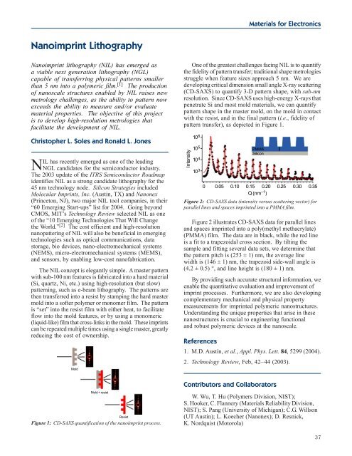
Figure 1: CD-SAXS quantification of the nanoimprint process.<br />
<strong>Materials</strong> for Electronics<br />
One of the greatest challenges facing NIL is to quantify<br />
the fidelity of pattern transfer; traditional shape metrologies<br />
struggle when feature sizes approach 5 nm. We are<br />
developing critical dimension small angle X-ray scattering<br />
(CD-SAXS) to quantify 3-D pattern shape, with sub-nm<br />
resolution. Since CD-SAXS uses high-energy X-rays that<br />
penetrate Si <strong>and</strong> most mold materials, we can quantify<br />
pattern shape in the master mold, on the mold in contact<br />
with the resist, <strong>and</strong> in the final pattern (i.e., fidelity of<br />
pattern transfer), as depicted in Figure 1.<br />
Figure 2: CD-SAXS data (intensity versus scattering vector) for<br />
parallel lines <strong>and</strong> spaces imprinted into a PMMA film.<br />
Figure 2 illustrates CD-SAXS data for parallel lines<br />
<strong>and</strong> spaces imprinted into a poly(methyl methacrylate)<br />
(PMMA) film. The data are in black, while the red line<br />
is a fit to a trapezoidal cross section. By tilting the<br />
sample <strong>and</strong> fitting several data sets, we determine that<br />
the pattern pitch is (253 ± 1) nm, the average line<br />
width is (146 ± 1) nm, the trapezoid side-wall angle is<br />
(4.2 ± 0.5) °, <strong>and</strong> line height is (180 ± 1) nm.<br />
By providing such accurate structural information, we<br />
enable the quantitative evaluation <strong>and</strong> improvement of<br />
imprint processes. Furthermore, we are also developing<br />
complementary mechanical <strong>and</strong> physical property<br />
measurements for imprinted polymeric nanostructures.<br />
Underst<strong>and</strong>ing the unique properties that arise in these<br />
nanostructures is crucial to engineering functional<br />
<strong>and</strong> robust polymeric devices at the nanoscale.<br />
References<br />
1. M.D. Austin, et al., Appl. Phys. Lett. 84, 5299 (<strong>2004</strong>).<br />
2. Technology Review, Feb, 42–44 (2003).<br />
Contributors <strong>and</strong> Collaborators<br />
W. Wu, T. Hu (Polymers Division, <strong>NIST</strong>);<br />
S. Hooker, C. Flannery (<strong>Materials</strong> Reliability Division,<br />
<strong>NIST</strong>); S. Pang (University of Michigan); C.G. Willson<br />
(UT Austin); L. Koecher (Nanonex); D. Resnick,<br />
K. Nordquist (Motorola)<br />
37