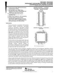
HIGH-SPEED 16K x 8 DUAL-PORT STATIC RAM
HIGH-SPEED 16K x 8 DUAL-PORT STATIC RAM
HIGH-SPEED 16K x 8 DUAL-PORT STATIC RAM
- No tags were found...

You also want an ePaper? Increase the reach of your titles
YUMPU automatically turns print PDFs into web optimized ePapers that Google loves.
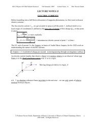
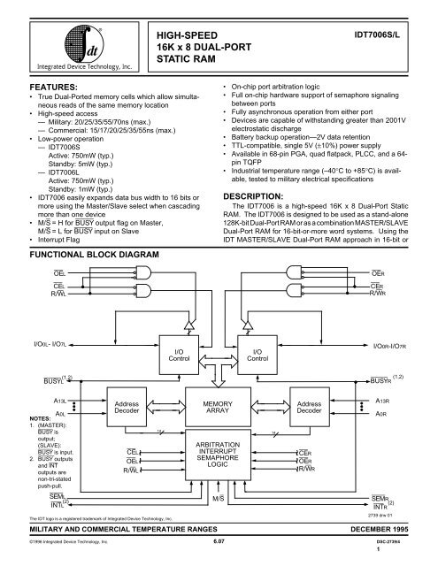
Integrated Device Technology, Inc.<strong>HIGH</strong>-<strong>SPEED</strong><strong>16K</strong> x 8 <strong>DUAL</strong>-<strong>PORT</strong><strong>STATIC</strong> <strong>RAM</strong>IDT7006S/LFEATURES:• True Dual-Ported memory cells which allow simultaneousreads of the same memory location• High-speed access— Military: 20/25/35/55/70ns (max.)— Commercial: 15/17/20/25/35/55ns (max.)• Low-power operation— IDT7006SActive: 750mW (typ.)Standby: 5mW (typ.)— IDT7006LActive: 750mW (typ.)Standby: 1mW (typ.)• IDT7006 easily expands data bus width to 16 bits ormore using the Master/Slave select when cascadingmore than one device• M/S = H for BUSY output flag on Master,M/S = L for BUSY input on Slave• Interrupt FlagFUNCTIONAL BLOCK DIAG<strong>RAM</strong>OELCELR/WL• On-chip port arbitration logic• Full on-chip hardware support of semaphore signalingbetween ports• Fully asynchronous operation from either port• Devices are capable of withstanding greater than 2001Velectrostatic discharge• Battery backup operation—2V data retention• TTL-compatible, single 5V (±10%) power supply• Available in 68-pin PGA, quad flatpack, PLCC, and a 64-pin TQFP• Industrial temperature range (–40°C to +85°C) is available,tested to military electrical specificationsDESCRIPTION:The IDT7006 is a high-speed <strong>16K</strong> x 8 Dual-Port Static<strong>RAM</strong>. The IDT7006 is designed to be used as a stand-alone128K-bit Dual-Port <strong>RAM</strong> or as a combination MASTER/SLAVEDual-Port <strong>RAM</strong> for 16-bit-or-more word systems. Using theIDT MASTER/SLAVE Dual-Port <strong>RAM</strong> approach in 16-bit orOERCERR/WRI/O0L- I/O7LI/OControlI/OControlI/O0R-I/O7RBUSYL(1,2) (1,2)BUSYRA13LA0LNOTES:1. (MASTER):BUSY isoutput;(SLAVE):BUSY is input.2. BUSY outputsand INToutputs arenon-tri-statedpush-pull.SEML(2)INTLAddressDecoderCELOELR/WLThe IDT logo is a registered trademark of Integrated Device Technology, Inc.14MEMORYARRAYARBITRATIONINTERRUPTSEMAPHORELOGICM/S14AddressDecoderCEROERR/WRA13RA0RSEMR(2)INTR2739 drw 01MILITARY AND COMMERCIAL TEMPERATURE RANGES DECEMBER 1995©1996 Integrated Device Technology, Inc. 6.07 DSC-2739/41
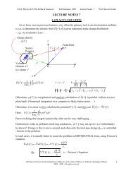
IDT7006S/L<strong>HIGH</strong>-<strong>SPEED</strong> <strong>16K</strong> x 8 <strong>DUAL</strong>-<strong>PORT</strong> <strong>STATIC</strong> <strong>RAM</strong>wider memory system applications results in full-speed, errorfreeoperation without the need for additional discrete logic.This device provides two independent ports with separatecontrol, address, and I/O pins that permit independent,asynchronous access for reads or writes to any location inmemory. An automatic power down feature controlled by CEpermits the on-chip circuitry of each port to enter a very lowstandby power mode.PIN CONFIGURATIONSMILITARY AND COMMERCIAL TEMPERATURE RANGESFabricated using IDT’s CMOS high-performance technology,these devices typically operate on only 750mW of power.Low-power (L) versions offer battery backup data retentioncapability with typical power consumption of 500µW from a 2Vbattery.The IDT7006 is packaged in a ceramic 68-pin PGA, an 68-pin quad flatpack, a PLCC, and a 64-pin thin plastic quadflatpack, TQFP. Military grade product is manufactured incompliance with the latest revision of MIL-STD-883, Class B,making it ideally suited to military temperature applicationsdemanding the highest level of performance and reliability.INDEXI/O2LI/O3LI/O4LI/O5LGNDI/O6LI/O7LVCCGNDI/O0RI/O1RI/O2RVCCI/O3RI/O4RI/O5RI/O6RI/O1LI/O0LN/COELR/WLSEMLCELN/C9 8 7 6 5 4 3 2 1 68 67 66 65 64 63 62 6110601159121358571456IDT700615J68-15516F68-15417531852PLCC / FLATPACK19TOP VIEW(1)51205021492248234724462545264427 28 29 30 31 32 33 34 35 36 37 38 39 40 41 42 43A13LVCCA12LA11LA10LA9LA8LA7LA6LA5LA4LA3LA2LA1LA0LINTLBUSYLGNDM/SBUSYRINTRA0RA1RA2RA3RA4RI/O7RN/COERR/WRSEMRCERN/CA13RGNDA12RNOTE:1. This text is does not indicate the actual part-markingA11RA10RA9RA8RA7RA6RA5R2739 drw 02INDEXI/O2LI/O3LI/O4LI/O5LGNDI/O6LI/O7LVCCGNDI/O0RI/O1RI/O2RVCCI/O3RI/O4RI/O5RI/O1L64123456789101112131415161718I/O6RI/O0LOEL6362I/O7RR/WL1920OERSEMLCEL6160595857565554R/WR2122SEMRVCC7006PN-64TQFPTOP VIEW(1)CERA13R A13L232425GNDA12LA12RA11L26A11RA10L2728A10RA9L5352A9RA8L512930A8RA7LA7RA6L5031A6RA5L4932A5R48474645444342414039383736353433A4LA3LA2LA1LA0LINTLBUSYLGNDM/SBUSYRINTRA0RA1RA2RA3RA4R2739 drw 036.07 2
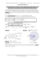
IDT7006S/L<strong>HIGH</strong>-<strong>SPEED</strong> <strong>16K</strong> x 8 <strong>DUAL</strong>-<strong>PORT</strong> <strong>STATIC</strong> <strong>RAM</strong>MILITARY AND COMMERCIAL TEMPERATURE RANGES111051 50 48 46 44 42 40 38 36A5LA4L A2L A0L BUSYL M/S INTR A1R A3R53 52 49 47 45 43 41 39 37 35 34A7L A6L A3L A1L INTL GND BUSYR A0R A2R A4R A5R0955A9L54A8L32A7R33A6R0857A11L56A10L30A9R31A8R07060559VCC61N/C63SEML58A12L60A13L62CELIDT7006G68-168-PIN PGATOP VIEW (3)28A11R26GND24N/C29A10R27A12R25A13R0465OEL64R/WL22SEMR23CER0367I/O0L66N/C20OER21R/WR020168 1 3 5 7 9 11 13 15 18 19I/O1L I/O2L I/O4L GND I/O7L GND I/O1R VCC I/O4R I/O7R N/C2 4 6 8 10 12 14 16 17I/O3L I/O5L I/O6L VCC I/O0R I/O2R I/O3R I/O5R I/O6RINDEXA B C D E F G H J K L2739 drw 04PIN NAMESLeft Port Right Port NamesCEL CER Chip EnableR/WL R/WR Read/Write EnableOEL OER Output EnableA0L – A13L A0R – A13R AddressI/O0L – I/O7L I/O0R – I/O7R Data Input/OutputSEML SEMR Semaphore EnableINTL INTR Interrupt FlagBUSYL BUSYR Busy FlagM/SMaster or Slave SelectVCCPowerGNDGround2739 tbl 01NOTES:1. All VCC pins must be connected to power supply.2. All GND pins must be connected to ground supply.3. This text does not indicate orientation of the actual part-marking6.07 3
IDT7006S/L<strong>HIGH</strong>-<strong>SPEED</strong> <strong>16K</strong> x 8 <strong>DUAL</strong>-<strong>PORT</strong> <strong>STATIC</strong> <strong>RAM</strong>MILITARY AND COMMERCIAL TEMPERATURE RANGESTRUTH TABLE: NON-CONTENTION READ/WRITE CONTROLInputs (1)OutputsCE R/W OESEM I/O0-7 ModeH X X H High-Z Deselected: Power-DownL L X H DATAIN Write to MemoryL H L H DATAOUT Read MemoryX X H X High-Z Outputs DisabledNOTE: 2739 tbl 021. A0L — A13L is not equal to A0R — A13RTRUTH TABLE: SEMAPHORE READ/WRITE CONTROL (1)InputsOutputsCE R/W OESEM I/O0-7 ModeH H L L DATAOUT Read Data in Semaphore Flag Data OutH u X L DATAIN Write I/O0 into Semaphore FlagL X X L — Not AllowedNOTE:1. There are eight semaphore flags written to via I/O0 and readfrom I/O0 - I/O15. These eight semaphores are addressed by A0 - A2.ABSOLUTE MAXIMUM RATINGS (1)Symbol Rating Commercial Military UnitVTERM (2) Terminal Voltage –0.5 to +7.0 –0.5 to +7.0 Vwith Respectto GNDTA Operating 0 to +70 –55 to +125 °CTemperatureTBIAS Temperature –55 to +125 –65 to +135 °CUnder BiasTSTG Storage –55 to +125 –65 to +150 °CTemperatureIOUT DC Output 50 50 mACurrentNOTES: 2739 tbl 041. Stresses greater than those listed under ABSOLUTE MAXIMUMRATINGS may cause permanent damage to the device. This is a stressrating only and functional operation of the device at these or any otherconditions above those indicated in the operational sections of thisspecification is not implied. Exposure to absolute maximum rating conditionsfor extended periods may affect reliability.2. VTERM must not exceed Vcc + 0.5V for more than 25% of the cycle timeor 10ns maximum, and is limited to < 20mA for the period of VTERM < Vcc+ 0.5V.RECOMMENDED OPERATINGTEMPERATURE AND SUPPLY VOLTAGERECOMMENDED DC OPERATINGCONDITIONS2739 tbl 03AmbientGrade Temperature GND VCCMilitary –55°C to +125°C 0V 5.0V ± 10%Commercial 0°C to +70°C 0V 5.0V ± 10%2739 tbl 05Symbol Parameter Min. Typ. Max. UnitVCC Supply Voltage 4.5 5.0 5.5 VGND Supply Voltage 0 0 0 VVIH Input High Voltage 2.2 — 6.0 (2) VVIL Input Low Voltage –0.5 (1) — 0.8 VNOTES: 2739 tbl 061. VIL≥ -1.5V for pulse width less than 10ns.2. VTERM must not exceed Vcc + 0.5V.CAPACITANCE (TA = +25°C, f = 1.0MHz)Symbol Parameter (1) Conditions Max. UnitCIN Input Capacitance VIN = 3dV 9 pFCOUT Output VOUT = 3dV 10 pFCapacitanceNOTE: 2739 tbl 071. This parameter is determined by device characterization, but is notproduction tested (TQFP Package Only).2. 3dv references the interpolated capacitance when the input and outputsignals switch from 0V to 3V or from 3V to 0V.6.07 4
IDT7006S/L<strong>HIGH</strong>-<strong>SPEED</strong> <strong>16K</strong> x 8 <strong>DUAL</strong>-<strong>PORT</strong> <strong>STATIC</strong> <strong>RAM</strong>MILITARY AND COMMERCIAL TEMPERATURE RANGESDC ELECTRICAL CHARACTERISTICS OVER THEOPERATING TEMPERATURE AND SUPPLY VOLTAGE RANGE (VCC = 5.0V ± 10%)IDT7006S IDT7006LSymbol Parameter Test Conditions Min. Max. Min. Max. Unit|ILI| Input Leakage Current (1) VCC = 5.5V, VIN = 0V to VCC — 10 — 5 µA|ILO| Output Leakage Current CE = VIH, VOUT = 0V to VCC — 10 — 5 µAVOL Output Low Voltage IOL = 4mA — 0.4 — 0.4 VVOH Output High Voltage IOH = -4mA 2.4 — 2.4 — VNOTE:1. At Vcc = 2.0V input leakages are undefined.2739 tbl 08DC ELECTRICAL CHARACTERISTICS OVER THEOPERATING TEMPERATURE AND SUPPLY VOLTAGE RANGE (1) (VCC = 5.0V ± 10%)7006X15 7006X17 7006X20 7006X25Test Com'l Only Com'l OnlySymbol Parameter Condition Version Typ. (2) Max. Typ. (2) Max. Typ. (2) Max. Typ. (2) Max. UnitICC Dynamic Operating CE < VIL, Outputs Open MIL. S — — — — 160 370 155 340 mACurrent SEM > VIH L — — — — 160 320 155 280(Both Ports Active) f = fMAX (3) COM. S 170 310 170 310 160 290 155 265L 170 260 170 260 160 240 155 220ISB1 Standby Current CEL = CER > VIH MIL. S — — — — 20 90 16 80 mA(Both Ports — TTL SEMR = SEML > VIH L — — — — 20 70 16 65Level Inputs f = fMAX (3) COM. S 20 60 20 60 20 60 16 60L 20 50 20 50 20 50 16 50ISB2 Standby Current CE"A"=VIL and CE"B"=VIH (5) MIL. S — — — — 95 240 90 215 mA(One Port — TTL Active Port Outputs Open L — — — — 95 210 90 180Level Inputs) f = fMAX (3) COM. S 105 190 105 190 95 180 90 170SEMR = SEML > VIH L 105 160 105 160 95 150 90 140ISB3 Full Standby Current Both Ports CEL and MIL. S — — — — 1.0 30 1.0 30 mA(Both Ports — All CER > VCC - 0.2V L — — — — — — 0.2 10CMOS Level Inputs) VIN > VCC - 0.2V or COM. S 1.0 15 1.0 15 1.0 15 1.0 15VIN < 0.2V, f = 0 (4) L 0.2 5 0.2 5 0.2 5 0.2 5SEMR = SEML > VCC-0.2VISB4 Full Standby Current CE"A" < 0.2V and MIL. S — — — — 90 225 85 200 mA(One Port — All CE"B" > VCC - 0.2V (5)CMOS Level Inputs) SEMR = SEML > VCC-0.2V L — — — — 90 200 85 170VIN > VCC - 0.2V or COM. S 100 170 100 170 90 155 85 145VIN < 0.2vActive Port Outputs Open, L 100 140 100 140 90 130 85 120f = fMAX (3)NOTES: 2739 tbl 091. "X" in part numbers indicates power rating (S or L)2. VCC = 5V, TA = +25°C, and are not production tested. ICC DC = 120mA (TYP)3. At f = fMAX, address and I/O'S are cycling at the maximum frequency read cycleof 1/tRC, and using “AC Test Conditions” of input levels of GND to 3V.4. f = 0 means no address or control lines change.5. Port "A"may be either left or right port. Port "B" is the port opposite port "A".6.07 5
IDT7006S/L<strong>HIGH</strong>-<strong>SPEED</strong> <strong>16K</strong> x 8 <strong>DUAL</strong>-<strong>PORT</strong> <strong>STATIC</strong> <strong>RAM</strong>MILITARY AND COMMERCIAL TEMPERATURE RANGESDC ELECTRICAL CHARACTERISTICS OVER THEOPERATING TEMPERATURE AND SUPPLY VOLTAGE RANGE (1) (Continued) (VCC = 5.0V ± 10%)7006X35 7006X55 7006X70TestMIL ONLYSymbol Parameter Condition Version Typ. (2) Max. Typ. (2) Max. Typ. (2) Max. UnitICC Dynamic Operating CE = VIL, Outputs Open MIL. S 150 300 150 300 140 300 mACurrent SEM = VIH L 150 250 150 250 140 250(Both Ports Active) f = fMAX (3) COM’L. S 150 250 150 250 — —L 150 210 150 210 — —ISB1 Standby Current CEL = CER = VIH MIL. S 13 80 13 80 10 80 mA(Both Ports — TTL SEMR = SEML = VIH L 13 65 13 65 10 65Level Inputs) f = fMAX (3) COM’L. S 13 60 13 60 — —L 13 50 13 50 — —ISB2 Standby Current CE"A"=VIL and CEL"B"=VIH (5) MIL. S 85 190 85 190 80 190 mA(One Port — TTL Active Port Outputs Open, L 85 160 85 160 80 160Level Inputs) f = fMAX (3) COM’L. S 85 155 85 155 — —SEMR = SEML = VIH L 85 130 85 130 — —ISB3 Full Standby Current Both Ports CEL and MIL. S 1.0 30 1.0 30 1.0 30 mA(Both Ports — All CER > VCC - 0.2V L 0.2 10 0.2 10 0.2 10CMOS Level Inputs) VIN > VCC - 0.2V or COM’L. S 1.0 15 1.0 15 — —VIN < 0.2V, f = 0 (4) L 0.2 5 0.2 5 — —SEMR = SEML≥ VCC - 0.2VISB4 Full Standby Current CE"A" < 0.2V and MIL. S 80 175 80 175 75 175 mA(One Port — All CE"B" > VCC - 0.2V (5)CMOS Level Inputs) SEMR = SEML≥ VCC - 0.2V L 80 150 80 150 75 150VIN > VCC - 0.2V or COM’L. S 80 135 80 135 — —VIN < 0.2VActive Port Outputs Open, L 80 110 80 110 — —f = fMAX (3)NOTES: 2739 tbl 101. 'X' in part numbers indicates power rating (S or L)2. VCC = 5V, TA = +25°C, and are not production tested. ICC DC =120ma (TYP)3. At f = fMAX, address and I/O'S are cycling at the maximum frequency read cycleof 1/tRC, and using “AC Test Conditions” of input levels of GND to 3V.4. f = 0 means no address or comtrol lines change.5. Port "A" may be either left or right port. Port "B"is the opposite from port "A".DATA RETENTION CHARACTERISTICS OVER ALL TEMPERATURE RANGES (L Version Only)(VLC = 0.2V, VHC = VCC - 0.2V) (4)Symbol Parameter Test Condition Min. Typ. (1) Max. UnitVDR VCC for Data Retention VCC = 2V 2.0 — — VICCDR Data Retention Current CE ≥ VHC MIL. — 100 4000 µAVIN ≥ VHC or ≤ VLC COM’L. — 100 1500tCDR (3) Chip Deselect to Data Retention Time SEM ≥ VHC 0 — — nstR (3) Operation Recovery Time tRC (2) — — nsNOTES: 2739 tbl 111. TA = +25°C, VCC = 2V, and are not production tested.2. tRC = Read Cycle Time3. This parameter is guaranteed by characterization, but are not production tested.4. At Vcc = 2V input leakages are undefinedDATA RETENTION WAVEFORMVCC4.5VDATA RETENTION MODEVDR ≥ 2V4.5VtCDRtRCEVIHVDRVIH2739 drw 056.07 6
IDT7006S/L<strong>HIGH</strong>-<strong>SPEED</strong> <strong>16K</strong> x 8 <strong>DUAL</strong>-<strong>PORT</strong> <strong>STATIC</strong> <strong>RAM</strong>MILITARY AND COMMERCIAL TEMPERATURE RANGESWAVEFORM OF READ CYCLES (5)tRCADDRCEOE(4)tAAtACE (4)tAOE (4)R/WDATAOUT(1)tLZVALID DATA (4)tOH(2)tHZBUSYOUT(3, 4)tBDD2739 drw 07NOTES:1. Timing depends on which signal is asserted last, OE or CE.2. Timing depends on which signal is de-asserted first CE or OE.3. tBDD delay is required only in cases where the opposite port is completing a write operation to the same address location. For simultaneous read operationsBUSY has no relation to valid output data.4. Start of valid data depends on which timing becomes effective last tAOE, tACE, tAA or tBDD.5. SEM = VIH.TIMING OF POWER-UP POWER-DOWNCEICCtPUtPDISB2739 drw 086.07 8
IDT7006S/L<strong>HIGH</strong>-<strong>SPEED</strong> <strong>16K</strong> x 8 <strong>DUAL</strong>-<strong>PORT</strong> <strong>STATIC</strong> <strong>RAM</strong>MILITARY AND COMMERCIAL TEMPERATURE RANGESAC ELECTRICAL CHARACTERISTICS OVER THEOPERATING TEMPERATURE AND SUPPLY VOLTAGE (5)DT7006X15 IDT7006X17 IDT7006X20 IDT7006X25Com'l Only Com'l OnlySymbol Parameter Min. Max. Min. Max. Min. Max. Min. Max. UnitWRITE CYCLEtWC Write Cycle Time 15 — 17 — 20 — 25 — nstEW Chip Enable to End-of-Write (3) 12 — 12 — 15 — 20 — nstAW Address Valid to End-of-Write 12 — 12 — 15 — 20 — nstAS Address Set-up Time (3) 0 — 0 — 0 — 0 — nstWP Write Pulse Width 12 — 12 — 15 — 20 — nstWR Write Recovery Time 0 — 0 — 0 — 0 — nstDW Data Valid to End-of-Write 10 — 10 — 15 — 15 — nstHZ Output High-Z Time (1, 2) — 10 — 10 — 12 — 15 nstDH Data Hold Time (4) 0 — 0 — 0 — 0 — nstWZ Write Enable to Output in High-Z (1, 2) — — — — — 12 — 15 nstOW Output Active from End-of-Write (1, 2, 4) 0 — 0 — 0 — 0 — nstSWRD SEM Flag Write to Read Time 5 — 5 — 5 — 5 — nstSPS SEM Flag Contention Window 5 — 5 — 5 — 5 — nsIDT7006X35 IDT7006X55 IDT7006X70MIL. ONLYSymbol Parameter Min. Max. Min. Max. Min. Max. UnitWRITE CYCLEtWC Write Cycle Time 35 — 55 — 70 — nstEW Chip Enable to End-of-Write (3) 30 — 45 — 50 — nstAW Address Valid to End-of-Write 30 — 45 — 50 — nstAS Address Set-up Time (3) 0 — 0 — 0 — nstWP Write Pulse Width 25 — 40 — 50 — nstWR Write Recovery Time 0 — 0 — 0 — nstDW Data Valid to End-of-Write 15 — 30 — 40 — nstHZ Output High-Z Time (1, 2) — 15 — 25 — 30 nstDH Data Hold Time (4) 0 — 0 — 0 — nstWZ Write Enable to Output in High-Z (1, 2) — 15 — 25 — 30 nstOW Output Active from End-of-Write (1, 2, 4) 0 — 0 — 0 — nstSWRD SEM Flag Write to Read Time 5 — 5 — 5 — nstSPS SEM Flag Contention Window 5 — 5 — 5 — nsNOTES: 2739 tbl 141. Transition is measured ±500mV from low or high impedance voltage with load (Figures 2).2. This parameter is guaranteed by device characterization, but is not production tested but not tested.3. To access <strong>RAM</strong>, CE = L, SEM = H. To access semaphore, CE = H and SEM = L. Either condition must be valid for the entire tEW time.4. The specification for tDH must be met by the device supplying write data to the <strong>RAM</strong> under all operating conditions. Although tDH and tOW values will varyover voltage and temperature, the actual tDH will always be smaller than the actual tOW.5. 'X' in part numbers indicates power rating (S or L).6.07 9
IDT7006S/L<strong>HIGH</strong>-<strong>SPEED</strong> <strong>16K</strong> x 8 <strong>DUAL</strong>-<strong>PORT</strong> <strong>STATIC</strong> <strong>RAM</strong>MILITARY AND COMMERCIAL TEMPERATURE RANGESTIMING WAVEFORM OF WRITE CYCLE NO. 1, R/W CONTROLLED TIMING (1,5,8)tWCADDRESSOEtHZ(7)CE or SEM (9)tAW(6)tAS(2)tWP(3)tWRR/WtWZ(7)tOWDATAOUT(4) (4)tDWtDHDATAINTIMING WAVEFORM OF WRITE CYCLE NO. 2, CE CONTROLLED TIMING (1,5)2739 drw 09tWCADDRESStAWCE or SEM(9)(6)tAStEW (2)(3)tWRR/WtDWtDHDATAIN2739 drw 10NOTES:1. R/W or CE must be high during all address transitions.2. A write occurs during the overlap (tEW or tWP) of a low CE and a low R/W for memory array writing cycle.3. tWR is measured from the earlier of CE or R/W (or SEM or R/W) going high to the end of write cycle.4. During this period, the I/O pins are in the output state and input signals must not be applied.5. If the CE or SEM low transition occurs simultaneously with or after the R/W low transition, the outputs remain in the high impedance state.6. Timing depends on which enable signal is asserted last, CE or R/W.7. This parameter is guaranteed by device characterization, but is not production tested. Transition is measured by +/- 500mV from steady state with theOutput Test Load (Figure 2)8. If OE is low during R/W controlled write cycle, the write pulse width must be the larger of tWP or (tWZ + tDW) to allow the I/O drivers to turn off and data tobe placed on the bus for the required tDW. If OE is high during an R/W controlled write cycle, this requirement does not apply and the write pulse can beas short as the specified tWP.9. To access <strong>RAM</strong>, CE = VIL and SEM = VIH. To access semaphore CE = VIH and SEM = VIL. tEW must be met for either condition.6.07 10
IDT7006S/L<strong>HIGH</strong>-<strong>SPEED</strong> <strong>16K</strong> x 8 <strong>DUAL</strong>-<strong>PORT</strong> <strong>STATIC</strong> <strong>RAM</strong>MILITARY AND COMMERCIAL TEMPERATURE RANGESTIMING WAVEFORM OF SEMAPHORE READ AFTER WRITE TIMING, EITHER SIDE (1)tSAAtOHA0-A2VALID ADDRESSVALID ADDRESStAWtWRtACESEMtEWtDWtSOPDATA0DATAINVALIDDATA OUTVALIDR/WtAStWPtDHtSWRDtAOEOEWrite CycleNOTE:1. CE = VIH for the duration of the above timing (both write and read cycle).tSOPRead Cycle2739 drw 11TIMING WAVEFORM OF SEMAPHORE WRITE CONTENTION (1,3,4)A0"A"-A2"A"MATCHSIDE(2)“A”R/W"A"SEM"A"tSPSA0"B"-A2"B"MATCHSIDE(2)“B”R/W"B"SEM"B"2739 drw 12NOTES:1. DOR = DOL = VIL, CER = CEL = VIH, Semaphore Flag is released from both sides (reads as ones from both sides) at cycle start.2. All timing is the same for left and right ports. Port “A” may be either left or right port. Port “B” is the opposite from port “A”.3. This parameter is measured from R/W"A" or SEM"A" going High to R/W"B" or SEM"B" going High.4. If tSPS is not satisfied, the semaphore will fall positively to one side or the other, but there is no guarantee which side will obtain the flag.6.07 11
IDT7006S/L<strong>HIGH</strong>-<strong>SPEED</strong> <strong>16K</strong> x 8 <strong>DUAL</strong>-<strong>PORT</strong> <strong>STATIC</strong> <strong>RAM</strong>AC ELECTRICAL CHARACTERISTICS OVER THEOPERATING TEMPERATURE AND SUPPLY VOLTAGE RANGE (6)BUSY TIMING (M/S = L)MILITARY AND COMMERCIAL TEMPERATURE RANGESIDT7006X15 IDT7006X17 IDT7006X20 IDT7006X25Com'l Only Com'l OnlySymbol Parameter Min. Max. Min. Max. Min. Max. Min. Max. UnitBUSY TIMING (M/S = H)tBAA BUSY Access Time from Address Match — 15 — 17 — 20 — 20 nstBDA BUSY Disable Time from Address Not Matched — 15 — 17 — 20 — 20 nstBAC BUSY Access Time from Chip Enable LOW — 15 — 17 — 20 — 20 nstBDC BUSY Disable Time from Chip Enable <strong>HIGH</strong> — 15 — 17 — 17 — 17 nstAPS Arbitration Priority Set-up Time (2) 5 — 5 — 5 — 5 — nstBDD BUSY Disable to Valid Data (3 — 15 — 17 — 20 — 25 nstWB BUSY Input to Write (4) 0 — 0 — 0 — 0 — nstWH Write Hold After BUSY (5) 12 — 13 — 15 — 17 — ns<strong>PORT</strong>-TO-<strong>PORT</strong> DELAY TIMINGtWDD Write Pulse to Data Delay (1) — 30 — 30 — 45 — 50 nstDDD Write Data Valid to Read Data Delay (1) — 25 — 25 — 35 — 35 nsIDT7006X35 IDT7006X55 IDT7006X70MIL. ONLYSymbol Parameter Min. Max. Min. Max. Min. Max. UnitBUSY TIMING (M/S = H)tBAA BUSY Access Time from Address Match — 20 — 45 — 45 nstBDA BUSY Disable Time from Address Not Matched — 20 — 40 — 40 nstBAC BUSY Access Time from Chip Enable LOW — 20 — 40 — 40 nstBDC BUSY Disable Time from Chip Enable <strong>HIGH</strong> — 20 — 35 — 35 nstAPS Arbitration Priority Set-up Time (2) 5 — 5 — 5 — nstBDD BUSY Disable to Valid Data (3) — 35 — 55 — 70 nstWH Write Hold After BUSY (5) 25 — 25 — 25 — nsBUSY TIMING (M/S = L)tWB BUSY Input to Write (4) 0 — 0 — 0 — nstWH Write Hold After BUSY (5) 25 — 25 — 25 — ns<strong>PORT</strong>-TO-<strong>PORT</strong> DELAY TIMINGtWDD Write Pulse to Data Delay (1) — 60 — 80 — 95 nstDDD Write Data Valid to Read Data Delay (1) — 45 — 65 — 80 nsNOTES: 2739 tbl 151. Port-to-port delay through <strong>RAM</strong> cells from writing port to reading port, refer to "Timing Waveform of Write with Port-to-Port Read and BUSY".2. To ensure that the earlier of the two ports wins.3. tBDD is a calculated parameter and is the greater of 0, tWDD – tWP (actual) or tDDD – tDW (actual).4. To ensure that the write cycle is inhibited with port "B" during contention on port "A".5. To ensure that a write cycle is completed on port "B" after contention with port "A".6. "X" is part numbers indicates power rating (S or L).6.07 12
IDT7006S/L<strong>HIGH</strong>-<strong>SPEED</strong> <strong>16K</strong> x 8 <strong>DUAL</strong>-<strong>PORT</strong> <strong>STATIC</strong> <strong>RAM</strong>MILITARY AND COMMERCIAL TEMPERATURE RANGESTIMING WAVEFORM OF WRITE WITH <strong>PORT</strong>-TO-<strong>PORT</strong> READ AND BUSY (2,5) (M/S = VIH)tWCADDR"A"MATCHtWPR/W"A"tDWtDHDATAIN "A"ADDR"B"(1)tAPSMATCHVALIDtBDAtBDDBUSY"B"tWDDDATAOUT "B"tDDD (3)NOTES:1. To ensure that the earlier of the two ports wins. tAPS is ignored for M/S = VIL (SLAVE).2. CEL = CER = VIL3. OE = ViL for the reading port.4. If M/S = VIL(slave) then BUSY is input (BUSY"A" = VIH and BUSY"B" = "don't care", for this example.5. All timing is the same for left and right port. Port "A' may be either left or right port. Port "B" is the port opposite from Port "A".VALID2739 drw 13TIMING WAVEFORM OF WRITE WITH BUSYtWPR/W"A"tWB(3)BUSY"B"tWH (1)R/W"B"NOTES:1. tWH must be met for both BUSY input (slave) and output (master).2. BUSY is asserted on Port "B" Blocking R/W"B", until BUSY"B" goes High.3. tWB is only for the 'Slave' Version.(2)2739 drw 146.07 13
IDT7006S/L<strong>HIGH</strong>-<strong>SPEED</strong> <strong>16K</strong> x 8 <strong>DUAL</strong>-<strong>PORT</strong> <strong>STATIC</strong> <strong>RAM</strong>MILITARY AND COMMERCIAL TEMPERATURE RANGESWAVEFORM OF BUSY ARBITRATION CONTROLLED BY CE TIMING (1) (M/S = H)ADDR"A"and "B"ADDRESSES MATCHCE"A"(2)tAPSCE"B"tBACtBDCBUSY"B"2739 drw 15WAVEFORM OF BUSY ARBITRATION CYCLE CONTROLLED BY ADDRESS MATCHTIMING (1) (M/S = H)ADDR"A"ADDRESS "N"(2)tAPSADDR"B"MATCHING ADDRESS "N"tBAAtBDABUSY"B"NOTES:1. All timing is the same for left and right ports. Port “A” may be either the left or right port. Port “B” is the port opposite from port “A”.2. If tAPS is not satisfied, the busy signal will be asserted on one side or another but there is no guarantee on which side busy will be asserted.AC ELECTRICAL CHARACTERISTICS OVER THEOPERATING TEMPERATURE AND SUPPLY VOLTAGE RANGE (1)2739 drw 16IDT7006X15 IDT7006X17 IDT7006X20 IDT7006X25Com'l Only Com'l OnlySymbol Parameter Min. Max. Min. Max. Min. Max. Min. Max. UnitINTERRUPT TIMINGtAS Address Set-up Time 0 — 0 — 0 — 0 — nstWR Write Recovery Time0 — 0 0 — 0 — 0 — nstINS Interrupt Set Time — 15 — 15 — 20 — 20 nstINR Interrupt Reset Time — 15 — 15 — 20 — 20 nsIDT7006X35 IDT7006X55 IDT7006X70MIL. ONLYSymbol Parameter Max. Min. Max. Min. Max. UnitINTERRUPT TIMINGtAS Address Set-up Time 0 — 0 — 0 — nstWR Write Recovery Time 0 — 0 — 0 — nstINS Interrupt Set Time — 25 — 40 — 50 nstINR Interrupt Reset Time — 25 — 40 — 50 nsNOTE: 2739 tbl 161. "X" in part numbers indicates power rating (S or L).6.07 14
IDT7006S/L<strong>HIGH</strong>-<strong>SPEED</strong> <strong>16K</strong> x 8 <strong>DUAL</strong>-<strong>PORT</strong> <strong>STATIC</strong> <strong>RAM</strong>MILITARY AND COMMERCIAL TEMPERATURE RANGESTRUTH TABLE II — ADDRESS BUSYARBITRATIONInputsA0L-A13LOutputsCELCER A0R-A13R BUSYL (1)BUSYR (1) FunctionX X NO MATCH H H NormalH X MATCH H H NormalX H MATCH H H NormalL L MATCH (2) (2) Write Inhibit (3)NOTES: 2739 tbl 181. Pins BUSYL and BUSYR are both outputs when the part is configured as a master. Both are inputs when configured as a slave. BUSYX outputs on theIDT7006 are push pull, not open drain outputs. On slaves the BUSYX input internally inhibits writes.2. "L" if the inputs to the opposite port were stable prior to the address and enable inputs of this port. "H" if the inputs to the opposite port became stableafter the address and enable inputs of this port. If tAPS is not met, either BUSYL or BUSYR = Low will result. BUSYL and BUSYR outputs cannot be lowsimultaneously.3. Writes to the left port are internally ignored when BUSYL outputs are driving low regardless of actual logic level on the pin. Writes to the right port areinternally ignored when BUSYR outputs are driving low regardless of actual logic level on the pin.TRUTH TABLE III — EXAMPLE OF SEMAPHORE PROCUREMENT SEQUENCE (1)(2)Functions D0 - D7 Left D0 - D7 Right StatusNo Action 1 1 Semaphore freeLeft Port Writes "0" to Semaphore 0 1 Left port has semaphore tokenRight Port Writes "0" to Semaphore 0 1 No change. Right side has no write access to semaphoreLeft Port Writes "1" to Semaphore 1 0 Right port obtains semaphore tokenLeft Port Writes "0" to Semaphore 1 0 No change. Left port has no write access to semaphoreRight Port Writes "1" to Semaphore 0 1 Left port obtains semaphore tokenLeft Port Writes "1" to Semaphore 1 1 Semaphore freeRight Port Writes "0" to Semaphore 1 0 Right port has semaphore tokenRight Port Writes "1" to Semaphore 1 1 Semaphore freeLeft Port Writes "0" to Semaphore 0 1 Left port has semaphore tokenLeft Port Writes "1" to Semaphore 1 1 Semaphore freeNOTES: 2739 tbl 191. This table denotes a sequence of events for only one of the eight semaphores on the IDT7006.2. There are eight semaphore flags written to via I/O0 and read from all I/O's. These eight semaphores are addressed by A0 - A2.FUNCTIONAL DESCRIPTIONThe IDT7006 provides two ports with separate control,address and I/O pins that permit independent access for readsor writes to any location in memory. The IDT7006 has anautomatic power down feature controlled by CE. The CEcontrols on-chip power down circuitry that permits therespective port to go into a standby mode when not selected(CE high). When a port is enabled, access to the entirememory array is permitted.INTERRUPTSIf the user chooses to use the interrupt function, a memorylocation (mail box or message center) is assigned to each port.The left port interrupt flag (INTL) is asserted when the right portwrites to memory location 3FFE (HEX) where a write isdefined as CE = R/W = VIL per the Truth Table . The left portclears the interrupt by reading address location 3FFE accesswhen CER = OER = VIL, R/W is a "don't care". Likewise, theright port interrupt flag (INTR) is asserted when the left portwrites to memory location 3FFF (HEX) and to clear theinterrupt flag (INTR), the right port must read the memorylocation 3FFF. The message (8 bits) at 3FFE or 3FFF is userdefined,since it is an addressable S<strong>RAM</strong> location. If theinterrupt function is not used, address locations 3FFE and3FFF are not used as mail boxes, but as part of the randomaccess memory. Refer to Table 1 for the interrupt operation.BUSY LOGICBusy Logic provides a hardware indication that both portsof the <strong>RAM</strong> have accessed the same location at the sametime. It also allows one of the two accesses to proceed andsignals the other side that the <strong>RAM</strong> is “busy”. The busy pin canthen be used to stall the access until the operation on the otherside is completed. If a write operation has been attemptedfrom the side that receives a busy indication, the write signalis gated internally to prevent the write from proceeding.The use of busy logic is not required or desirable for allapplications. In some cases it may be useful to logically OR6.07 16
IDT7006S/L<strong>HIGH</strong>-<strong>SPEED</strong> <strong>16K</strong> x 8 <strong>DUAL</strong>-<strong>PORT</strong> <strong>STATIC</strong> <strong>RAM</strong>MILITARY AND COMMERCIAL TEMPERATURE RANGESMASTER CEDual Port<strong>RAM</strong>BUSY (L) BUSY (R)SLAVE CEDual Port<strong>RAM</strong>BUSY (L) BUSY (R)DECODERBUSY (L)MASTER CEDual Port<strong>RAM</strong>BUSY (L) BUSY (R)SLAVEDual Port<strong>RAM</strong>BUSY (L)CEBUSY (R)BUSY (R)2739 drw 19Figure 3. Busy and chip enable routing for both width and depth expansion with IDT7006 <strong>RAM</strong>s.the busy outputs together and use any busy indication as aninterrupt source to flag the event of an illegal or illogicaloperation. If the write inhibit function of busy logic is notdesirable, the busy logic can be disabled by placing the part inslave mode with the M/S pin. Once in slave mode the BUSYpin operates solely as a write inhibit input pin. Normal operationcan be programmed by tying the BUSY pins high. Ifdesired, unintended write operations can be prevented to aport by tying the busy pin for that port low.The busy outputs on the IDT 7006 <strong>RAM</strong> in master mode,are push-pull type outputs and do not require pull up resistorsto operate. If these <strong>RAM</strong>s are being expanded in depth, thenthe busy indication for the resulting array requires the use ofan external AND gate.WIDTH EXPANSION WITH BUSY LOGICMASTER/SLAVE ARRAYSWhen expanding an IDT7006 <strong>RAM</strong> array in width whileusing busy logic, one master part is used to decide which sideof the <strong>RAM</strong>s array will receive a busy indication, and to outputthat indication. Any number of slaves to be addressed in thesame address range as the master, use the busy signal as awrite inhibit signal. Thus on the IDT7006 <strong>RAM</strong> the busy pin isan output if the part is used as a master (M/S pin = H), and thebusy pin is an input if the part used as a slave (M/S pin = L) asshown in Figure 3.If two or more master parts were used when expanding inwidth, a split decision could result with one master indicatingbusy on one side of the array and another master indicatingbusy on one other side of the array. This would inhibit the writeoperations from one port for part of a word and inhibit the writeoperations from the other port for the other part of the word.The busy arbitration, on a master, is based on the chipenable and address signals only. It ignores whether an accessis a read or write. In a master/slave array, both address andchip enable must be valid long enough for a busy flag to beoutput from the master before the actual write pulse can beinitiated with the R/W signal. Failure to observe this timing canresult in a glitched internal write inhibit signal and corrupteddata in the slave.SEMAPHORESThe IDT7006 is an extremely fast Dual-Port <strong>16K</strong> x 8 CMOSStatic <strong>RAM</strong> with an additional 8 address locations dedicatedto binary semaphore flags. These flags allow either processoron the left or right side of the Dual-Port <strong>RAM</strong> to claim aprivilege over the other processor for functions defined by thesystem designer’s software. As an example, the semaphorecan be used by one processor to inhibit the other fromaccessing a portion of the Dual-Port <strong>RAM</strong> or any other sharedresource.The Dual-Port <strong>RAM</strong> features a fast access time, and bothports are completely independent of each other. This meansthat the activity on the left port in no way slows the access timeof the right port. Both ports are identical in function to standardCMOS Static <strong>RAM</strong> and can be read from, or written to, at thesame time with the only possible conflict arising from thesimultaneous writing of, or a simultaneous READ/WRITE of,a non-semaphore location. Semaphores are protected againstsuch ambiguous situations and may be used by the systemprogram to avoid any conflicts in the non-semaphore portionof the Dual-Port <strong>RAM</strong>. These devices have an automaticpower-down feature controlled by CE, the Dual-Port <strong>RAM</strong>enable, and SEM, the semaphore enable. The CE and SEMpins control on-chip power down circuitry that permits therespective port to go into standby mode when not selected.This is the condition which is shown in Truth Table where CEand SEM are both high.Systems which can best use the IDT7006 contain multipleprocessors or controllers and are typically very high-speedsystems which are software controlled or software intensive.These systems can benefit from a performance increaseoffered by the IDT7006s hardware semaphores, which providea lockout mechanism without requiring complex programming.Software handshaking between processors offers themaximum in system flexibility by permitting shared resourcesto be allocated in varying configurations. The IDT7006 doesnot use its semaphore flags to control any resources throughhardware, thus allowing the system designer total flexibility insystem architecture.6.07 17
IDT7006S/L<strong>HIGH</strong>-<strong>SPEED</strong> <strong>16K</strong> x 8 <strong>DUAL</strong>-<strong>PORT</strong> <strong>STATIC</strong> <strong>RAM</strong>be handled via the initialization program at power-up. Sinceany semaphore request flag which contains a zero must bereset to a one, all semaphores on both sides should have aone written into them at initialization from both sides to assurethat they will be free when needed.USING SEMAPHORES—SOME EXAMPLESPerhaps the simplest application of semaphores is theirapplication as resource markers for the IDT7006’s Dual-Port<strong>RAM</strong>. Say the <strong>16K</strong> x 8 <strong>RAM</strong> was to be divided into two 8K x8 blocks which were to be dedicated at any one time toservicing either the left or right port. Semaphore 0 could beused to indicate the side which would control the lower sectionof memory, and Semaphore 1 could be defined as theindicator for the upper section of memory.To take a resource, in this example the lower 8K ofDual-Port <strong>RAM</strong>, the processor on the left port could write andthen read a zero in to Semaphore 0. If this task were successfullycompleted (a zero was read back rather than a one), theleft processor would assume control of the lower 8K. Meanwhilethe right processor was attempting to gain control of theresource after the left processor, it would read back a one inresponse to the zero it had attempted to write into Semaphore0. At this point, the software could choose to try and gaincontrol of the second 8K section by writing, then reading a zerointo Semaphore 1. If it succeeded in gaining control, it wouldlock out the left side.Once the left side was finished with its task, it would writea one to Semaphore 0 and may then try to gain access toSemaphore 1. If Semaphore 1 was still occupied by the rightside, the left side could undo its semaphore request andperform other tasks until it was able to write, then read a zerointo Semaphore 1. If the right processor performs a similartask with Semaphore 0, this protocol would allow the twoprocessors to swap 8K blocks of Dual-Port <strong>RAM</strong> with eachMILITARY AND COMMERCIAL TEMPERATURE RANGESother.The blocks do not have to be any particular size and caneven be variable, depending upon the complexity of thesoftware using the semaphore flags. All eight semaphorescould be used to divide the Dual-Port <strong>RAM</strong> or other sharedresources into eight parts. Semaphores can even be assigneddifferent meanings on different sides rather than beinggiven a common meaning as was shown in the exampleabove.Semaphores are a useful form of arbitration in systems likedisk interfaces where the CPU must be locked out of a sectionof memory during a transfer and the I/O device cannot tolerateany wait states. With the use of semaphores, once the twodevices has determined which memory area was “off-limits” tothe CPU, both the CPU and the I/O devices could access theirassigned portions of memory continuously without any waitstates.Semaphores are also useful in applications where nomemory “WAIT” state is available on one or both sides. Oncea semaphore handshake has been performed, both processorscan access their assigned <strong>RAM</strong> segments at full speed.Another application is in the area of complex data structures.In this case, block arbitration is very important. For thisapplication one processor may be responsible for building andupdating a data structure. The other processor then readsand interprets that data structure. If the interpreting processorreads an incomplete data structure, a major error conditionmay exist. Therefore, some sort of arbitration must be usedbetween the two different processors. The building processorarbitrates for the block, locks it and then is able to go in andupdate the data structure. When the update is completed, thedata structure block is released. This allows the interpretingprocessor to come back and read the complete data structure,thereby guaranteeing a consistent data structure.L <strong>PORT</strong>SEMAPHOREREQUEST FLIP FLOPR <strong>PORT</strong>SEMAPHOREREQUEST FLIP FLOPD0WRITEDQQDD0WRITESEMAPHOREREADSEMAPHOREREAD2739 drw 20Figure 4. IDT7006 Semaphore Logic6.07 19
IDT7006S/L<strong>HIGH</strong>-<strong>SPEED</strong> <strong>16K</strong> x 8 <strong>DUAL</strong>-<strong>PORT</strong> <strong>STATIC</strong> <strong>RAM</strong>MILITARY AND COMMERCIAL TEMPERATURE RANGESORDERING INFORMATIONIDTXXXXXA999AADeviceTypePowerSpeedPackageProcess/TemperatureRangeBlankBPFGJFCommercial (0°C to +70°C)Military (–55°C to +125°C)Compliant to MIL-STD-883, Class B64-pin TQFP (PN64-1)68-pin PGA (G68-1)68-pin PLCC (J68-1)68-pin Flatpack (F68-1)15172025355570SLCommercial OnlyCommercial OnlyMilitary OnlyStandard PowerLow PowerSpeed in nanoseconds7006128K (<strong>16K</strong> x 8) Dual-Port <strong>RAM</strong>2739 drw 216.07 20