Sentaurus Device Optoelectronics Datasheet - Europractice
Sentaurus Device Optoelectronics Datasheet - Europractice
Sentaurus Device Optoelectronics Datasheet - Europractice
- No tags were found...

You also want an ePaper? Increase the reach of your titles
YUMPU automatically turns print PDFs into web optimized ePapers that Google loves.
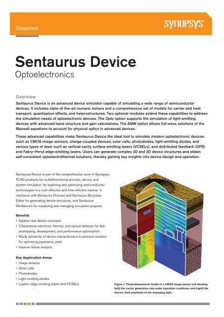
<strong>Datasheet</strong><strong>Sentaurus</strong> <strong>Device</strong><strong>Optoelectronics</strong>Overview<strong>Sentaurus</strong> <strong>Device</strong> is an advanced device simulator capable of simulating a wide range of semiconductordevices. It includes state-of-the-art numeric solvers and a comprehensive set of models for carrier and heattransport, quantization effects, and heterostructures. Two optional modules extend these capabilities to addressthe simulation needs of optoelectronic devices. The Opto option supports the simulation of light-emittingdevices with advanced band structure and gain calculations. The EMW option allows full-wave solutions of theMaxwell equations to account for physical optics in advanced devices.These advanced capabilities make <strong>Sentaurus</strong> <strong>Device</strong> the ideal tool to simulate modern optoelectronic devicessuch as CMOS image sensors, charge-coupled devices, solar cells, photodiodes, light-emitting diodes, andvarious types of laser such as vertical-cavity surface-emitting lasers (VCSELs), and distributed feedback (DFB)and Fabry–Perot edge-emitting lasers. Users can generate complex 2D and 3D device structures and obtainself-consistent optoelectrothermal solutions, thereby gaining key insights into device design and operation.<strong>Sentaurus</strong> <strong>Device</strong> is part of the comprehensive suite of SynopsysTCAD products for multidimensional process, device, andsystem simulation, for exploring and optimizing semiconductortechnologies in a cost-effective and time-efficient manner. Itinterfaces with <strong>Sentaurus</strong> Process and <strong>Sentaurus</strong> StructureEditor for generating device structures, and <strong>Sentaurus</strong>Workbench for visualizing and managing simulation projects.Benefits• Explore new device concepts• Characterize electrical, thermal, and optical behavior for fastprototyping, development, and performance optimization• Study sensitivity of device characteristics to process variationfor optimizing parametric yield• Improve failure analysisKey Application Areas• Image sensors• Solar cells• Photodiodes• Light-emitting diodes• Lasers: edge-emitting lasers and VCSELsFigure 1: Three-dimensional model of a CMOS image sensor cell showing(left) the carrier generation rate under operation conditions and (right) theelectric field amplitude of the impinging light.06-14355_sdeviceopto_ds.indd 18/31/2006 10:43:08 AM
<strong>Sentaurus</strong> <strong>Device</strong> <strong>Optoelectronics</strong>65RESETVoltage [V]4321DARKILLUMINATED05e-05 0.0001Time [s]Figure 2: (Left) Four-pixel structure usedfor TCAD simulation of CMOS imagesensors, (upper right) transient voltageresponse from device simulation of onepixel for dark and illuminated conditions,and (lower right) steady-state absoluteoptical field inside a 2D cross section ofthe device for an obliquely incident planewave.Image SensorsContinued scaling of CMOS technologies and the drive todecrease pixel size have made the design of CMOS imagesensors increasingly complex. TCAD plays a significant role in thedesign of image sensors by allowing scientists and engineers tosimulate critical aspects of the process and device design.Standard CMOS process steps such as silicidation can have anadverse impact on image sensor photosensitivity. Therefore, itis often necessary to optimize the process flow to tailor specificimage sensor performance targets, a task for which TCAD isideally suited.As pixels in modern image sensors are of comparable dimensionto the wavelength of light, diffraction, polarization, andinterference effects become important, requiring full-wave opticalsimulation. Moreover, by combining multiple pixels into a singlesimulation, optical and electrical crosstalk for normal and obliqueincidence can be analyzed.When a TCAD model of the image sensor is developed, the effectof manufacturing tolerances on sensor performance, such as lensmisalignment, can be quantified in ways that are impractical oreven impossible without simulation.In summary, <strong>Sentaurus</strong> <strong>Device</strong> supports image sensor designfrom concept to manufacturing, leading to higher performanceproducts and shorter time-to-market.Optical Solvers• 1D transfer matrix method• 2D and 3D raytracing with multilayer antireflection model• 2D and 3D beam propagation method• 2D and 3D parallelized finite-difference time-domain (FDTD)solver• Different meshes for optics and electrical transport tooptimize simulation speedSpecific Physics• Industry and process-calibrated silicon data• Direct interface to the <strong>Sentaurus</strong> Process simulator• Advanced generation and recombination modelsFocused Results• Doping profile optimization• Lens and geometry optimization• Crosstalk and pixel vignetting analysis• Spectral responsivity• Charge-voltage conversion, saturation effects• Capacitance extraction• Dark and light I–V analysis• Electrical AC and transient responses• Internal and external quantum efficiencies06-14355_sdeviceopto_ds.indd 28/31/2006 10:43:09 AM
<strong>Sentaurus</strong> <strong>Device</strong> <strong>Optoelectronics</strong>10080EQE, IQE [%]604020IQEEQE0400 600 800 1000Wavelength [nm]Figure 4: Internal quantum efficiency andexternal quantum efficiency for a siliconsolar cell.Optical Generation1.0e+211.0e+201.0e+191.0e+181.0e+171.0e+16Figure 3: Three-dimensional model of aninverted pyramid structure on a solar cellshowing (lines) the raytracing results and(contour) the optical generation rate.Figure 5: Parallel coordinate plot of process compactmodel describing main solar cell characteristics forparameter variation of substrate thickness, back-contactwidth, and back-surface recombination velocity. Each linecorresponds to one experiment.Solar CellsOptimizing the efficiency of a solar cell is a major challengewherein simulation is a powerful tool for quantifying andminimizing the losses that limit cell efficiency. This is madepossible by the advanced electrical and optical models of<strong>Sentaurus</strong> <strong>Device</strong>.The wide-ranging capabilities in <strong>Sentaurus</strong> <strong>Device</strong> have beensuccessfully demonstrated in numerous publications addressingvarious types of solar cell including monocrystalline silicon,multicrystalline silicon, and thin films using II–VI and III–Vcompound semiconductors. TCAD simulations allow designersto gain physical insights into solar cell operation, from carriertransport and recombination in the grain boundaries of CIGS andCdTe cells to optimization of the epitaxial layers in multijunctionhigh-efficiency cells for concentrator systems.To date, the application of TCAD to solar cells has focusedon device simulation. Yet, there is a vast body of knowledge inprocess simulation of CMOS technologies that is applicable tothe process optimization of photovoltaic technologies. Detailedprocess models including diffusion and gettering effectscan track the evolution of doping and lifetime profiles duringfabrication using <strong>Sentaurus</strong> Process, resulting in realistic processstructures for electrical analysis in <strong>Sentaurus</strong> <strong>Device</strong>.Optical Solvers• 1D transfer matrix method• 2D and 3D raytracing with multilayer antireflection model• 2D and 3D beam propagation method• 2D and 3D parallelized FDTD solver• Different meshes for optics and electrical transport tooptimize simulation speedSpecific Physics• Combine device simulation with process modeling,considering diffusion and gettering effects• Wavelength-dependent optical properties• Spectral optical generation• Support for compound materials and heterostructuresFocused Results• Compute illuminated and dark I–V characteristics• Extract internal and external quantum efficiencies• Optimize reflection spectra• Investigate perimeter losses• Maximize light trapping• Examine arbitrary 3D textures06-14355_sdeviceopto_ds.indd 38/31/2006 10:43:10 AM
<strong>Sentaurus</strong> <strong>Device</strong> <strong>Optoelectronics</strong>AR CoatingAnnular ContactArea100918273645546372819100.5 0.65 0.8 0.95 1.1 1.25 1.4 1.55 1.7 1.85 2ThicknessResponsivity [A/W]0.50.40.30.20.10Noncoherent Optical ModelCoherent Optical Model5e-07 1e-06Wavelength [m]Current [A]10 -5 150 K10 -6 140 K130 K120 K10 -7110 K100 K10 -810 -910 -1060 K10 -1110 -1290 K80 K70 K0.2 0.4 0.6 0.8 1Reverse Bias [V]Figure 6: (Upper left) Typical mesa structureused for InGaAs/InP TCAD simulation, (upperright) responsivity–band width ‘processwindow’ derived from geometry (area,depletion region thickness) variation in avertical photodiode, (lower left) illustration ofthe effect of coherent optics on responsivity insubmicron photodiodes, and (lower right) darkcurrent variation as a function of temperaturein HgCdTe photodiodes.PhotodiodesThe three major device characteristics of photodiodes arespectral responsivity, dark current, and band width. Accurateoptical models are required to describe spectral responsivity,which exhibits full-wave (coherent) effects in submicronstructures. Analysis of the different sources of dark current isoften a crucial task in photodiode design. The band width ofa photodiode is determined by the transient carrier transport.A comprehensive simulation approach based on TCAD,which incorporates optical, thermal, and electrical aspects oftransport, is crucial for the analysis and design of state-of-the-artphotodiode devices.Optical Solvers• 1D transfer matrix method• 2D and 3D raytracing with multilayer antireflection model• 2D and 3D beam propagation method• 2D and 3D parallelized FDTD solverSpecific Physics• Combine device simulation with process modeling for CMOSphotodiodes• Spectral optical generation• Wavelength-dependent optical properties• Support for compound materials and heterostructures• Accurate temperature-dependent models for band gap,mobilities, and tunneling for HgCdTe photodiodes• Calibrated drift-diffusion model for InGaAs/InP photodiodesFocused Results• Compute illuminated and dark I–V characteristics• Optimize spectral responsivity• Extract reflection spectra• Investigate perimeter losses• Investigate temperature dependence of dark current(especially for HgCdTe)• Simulate pulse response and extract the band width06-14355_sdeviceopto_ds.indd 48/31/2006 10:43:13 AM
<strong>Sentaurus</strong> <strong>Device</strong> <strong>Optoelectronics</strong>ExternalReflectorFigure 8: Special reflective boundary condition can be attached to arbitrary surfacesto model external optics: (left) corresponding raytree of (right) ATON-like 3D structurewith external spherical reflector.Figure 7: Major design parameters such as (top)temperature distribution and (bottom) current pathscan be investigated easily.Figure 9: Complex structures can begenerated using <strong>Sentaurus</strong> StructureEditor; a truncated pyramid structurewith a dome lens is shown.Light-Emitting DiodesThe relatively large dimensions of light-emitting diodes (LEDs),typically in the millimeter range, motivate the use of efficientraytracing models for the optical problem. Given the complexgeometry of modern-day LEDs, it is essential that the interactionbetween the optics and carrier transport is carried out in 2Dor 3D self-consistently: The carrier transport provides the lightemission source to be used in raytracing, while raytracing givesa photon-recycling recombination rate to be fed back into thecarrier transport.Optical Solvers• 2D and 3D raytracing with multilayer antireflection model• Flexible boundary condition in raytracing to define packagingcomponents• Different meshes for optics and electrical transport to optimizespeed of simulationSpecific Physics• Advanced physical models for photon recycling, includingamplified spontaneous emission and spontaneous spectrumincorporated within raytracing• Carrier density, wavelength-dependent, and temperaturedependentrefractive index model• Advanced carrier capture physics in quantum wells (QWs)• Different gain tables for different QWs in multiple–quantumwell devices (see page 7)Focused Results• Light power versus current• LED far-field radiation pattern design• Spectrum output design• Extraction efficiency optimization• Internal quantum efficiency optimization• Current spreading optimization• Geometry and electrical contact design optimization• Thermal analysis and management• Electrostatic discharge (ESD) simulation06-14355_sdeviceopto_ds.indd 58/31/2006 10:43:14 AM
<strong>Sentaurus</strong> <strong>Device</strong> <strong>Optoelectronics</strong>Relative Intensity Noise [dB/Hz]-90-95-100-105-110-115-120-125I = I th + 0.25 mAI = I th + 1.25 mAI = I th + 2.25 mA-130Simulation-135Measurement-1400 1 2 3 4 5 6 7 8Frequency [GHz]Figure 11: Example of typical laser characteristics forAlGaAs VCSEL, showing relative intensity noise versusfrequency.Figure 10: Optical intensity profileof fundamental HE11 mode ofan oxide-confined vertical-cavitysurface-emitting laser (VCSEL).0102030Rear Mirror [mA]4050601020304050Front Mirror [mA]156015400Wavelength [nm]Figure 12: Wavelength map for a widely tunablesampled-grating distributed Bragg reflector (SGDBR)laser; by tuning front and rear currents of DBR mirrors,the reflection peak and, therefore, lasing wavelengthcan be tuned in large discrete steps or in a finecontinuous way.LasersThe physics of semiconductor lasers is very complex due tothe strong interaction between the light field and the chargecarriers. <strong>Sentaurus</strong> <strong>Device</strong> addresses the two key factors forsuccessful simulation of semiconductor devices: (a) the useof comprehensive physical models for optical effects, carriertransport, self-heating, gain, and band structure calculation, and(b) the robust and self-consistent numeric coupling of all models,which allows fast and accurate simulations.Combined with the flexible structure-editing tool <strong>Sentaurus</strong>Structure Editor, the advanced models and numeric solversin <strong>Sentaurus</strong> <strong>Device</strong> enable the simulation of various laserssuch as VCSELs, and distributed feedback and Fabry–Perotedge-emitting lasers (EELs) in 2D and 3D. These simulationscan be used for yield analysis with <strong>Sentaurus</strong> TFM, therebyproviding users with a complete Design for Manufacturing (DFM)environment.Optical Solvers• Scalar finite-element method (for EELs)• Vectorial finite-element method (for EELs and VCSELs)• Effective index method (for VCSELs)• Transfer matrix method (for VCSELs)• Different meshes for optics and electrical transport to optimizespeed of simulationSpecific Physics• Coupled multiple lasing modes• Efficient link to the advanced band structure and gaincalculation module (see page 7)• Different gain tables for different QWs in multiple–quantumwell devices (see page 7)• Fully self-consistent solution of optics, electronic transport,self-heating, and band structure calculation• Comprehensive free carrier absorption models• Carrier density, wavelength-dependent, and temperaturedependentrefractive index modelFocused Results• Light–current–voltage (L–I–V) curves• Power spectrum• Mode competition analysis• Leaky waveguide laser design• Multiple QWs and gain design• Internal quantum efficiency optimization• Wavelength tuning• Near-field and far-field design• Spatial hole-burning• Self-heating and thermal rollover analysis• Thermal management and reduction of hot spots• Transient simulation• Small-signal modulation response• Relative intensity noise analysis• Line-width broadening06-14355_sdeviceopto_ds.indd 68/31/2006 10:43:17 AM
<strong>Sentaurus</strong> <strong>Device</strong> <strong>Optoelectronics</strong>5040SimulationExperiment0Conduction BandModal Gain [cm -1 ]3020100-102.95 3 3.05Energy [eV]Energy [eV]-1-2-3Electron WaveHeavy Hole WaveValence Band1e-08 1.5e-08Vertical Position [m]No Piezo ChargePiezo Charge = 5e13Figure 13: Modal gain versus transmission energy for a laser device withInGaN/GaN quantum wells.Figure 14: Band diagrams and wavefunctions of an InGaN/GaNquantum well (red) with and (blue) without piezoelectric charges atthe quantum well interfaces; piezoelectric charges lead to tilting ofthe quantum well, resulting in separation of wavefunctions, therebyreducing their overlap integrals and the stimulated emission rate.Advanced Band Structure and Gain CalculationFor LED and laser applications, an accurate model of theoptical emission process is crucially important for successfulsimulations. In particular, photoluminescence, absorption,material gain, and spontaneous emission are key elements thatdetermine the performance of active devices. The calculation ofthese processes requires the use of accurate electronic bandstructures and comprehensive emission models.<strong>Sentaurus</strong> <strong>Device</strong> includes both an advanced k.p bandstructure calculation and a gain model based on state-of-the-artquantum-mechanical manybody theory, allowing users to predictaccurately the optical properties of an active material. Dependingon the approximation chosen by the user, no specification ofphenomenological parameters is necessary for calculating theline-shape broadening and the charge-carrier dephasing rates.Specific Physics• Advanced 4x4, 6x6, and 8x8 k.p model for QW zinc-blendeand wurtzite band structure and gain calculations• Piezoelectric charge modeling and screening for strainedGaN QWs• Manybody effects in gain based on free carrier theory(FCT), screened Hartree–Fock (SHF), or second Bornapproximation• Lorentzian, Landsberg, and hyperbolic cosine gainbroadeningmodels for FCT and SHF approximationsFocused Results• Material gain spectra• Spontaneous emission spectra• Absorption spectra• Electron and hole wavefunctions• Calibration of Hakki–Paoli gain measurements• Designing gain spectra of multiple–quantum well devices• Generation of gain tables depending on carrier densities,energy, and temperature06-14355_sdeviceopto_ds.indd 78/31/2006 10:43:18 AM