NUCLEATION AND GROWTH OF Cu THIN FILMS ON SILICON ...
NUCLEATION AND GROWTH OF Cu THIN FILMS ON SILICON ...
NUCLEATION AND GROWTH OF Cu THIN FILMS ON SILICON ...
- No tags were found...

Create successful ePaper yourself
Turn your PDF publications into a flip-book with our unique Google optimized e-Paper software.
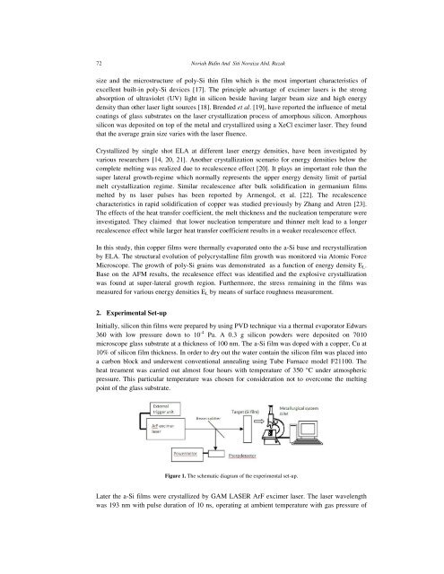
72 Noriah Bidin And Siti Noraiza Abd. Razaksize and the microstructure of poly-Si thin film which is the most important characteristics ofexcellent built-in poly-Si devices [17]. The principle advantage of excimer lasers is the strongabsorption of ultraviolet (UV) light in silicon beside having larger beam size and high energydensity than other laser light sources [18]. Brended et al. [19], have reported the influence of metalcoatings of glass substrates on the laser crystallization process of amorphous silicon. Amorphoussilicon was deposited on top of the metal and crystallized using a XeCl excimer laser. They foundthat the average grain size varies with the laser fluence.Crystallized by single shot ELA at different laser energy densities, have been investigated byvarious researchers [14, 20, 21]. Another crystallization scenario for energy densities below thecomplete melting was realized due to recalescence effect [20]. It plays an important role than thesuper lateral growth-regime which normally represents the upper energy density limit of partialmelt crystallization regime. Similar recalescence after bulk solidification in germanium filmsmelted by ns laser pulses has been reported by Armengol, et al. [22]. The recalescencecharacteristics in rapid solidification of copper was studied previously by Zhang and Atren [23].The effects of the heat transfer coefficient, the melt thickness and the nucleation temperature wereinvestigated. They claimed that lower nucleation temperature and thinner melt lead to a longerrecalescence effect while larger heat transfer coefficient results in a weaker recalescence effect.In this study, thin copper films were thermally evaporated onto the a-Si base and recrystallizationby ELA. The structural evolution of polycrystalline film growth was monitored via Atomic ForceMicroscope. The growth of poly-Si grains was demonstrated as a function of energy density E L .Base on the AFM results, the recalesence effect was identified and the explosive crystallizationwas found at super-lateral growth region. Furthermore, the stress remaining in the films wasmeasured for various energy densities E L by means of surface roughness measurement.2. Experimental Set-upInitially, silicon thin films were prepared by using PVD technique via a thermal evaporator Edwars360 with low pressure down to 10 -4 Pa. A 0.3 g silicon powders were deposited on 7010microscope glass substrate at a thickness of 100 nm. The a-Si film was doped with a copper, <strong>Cu</strong> at10% of silicon film thickness. In order to dry out the water contain the silicon film was placed intoa carbon block and underwent conventional annealing using Tube Furnace model F21100. Theheat treament was carried out almost four hours with temperature of 350 °C under atmosphericpressure. This particular temperature was chosen for consideration not to overcome the meltingpoint of the glass substrate.Figure 1. The schematic diagram of the experimental set-up.Later the a-Si films were crystallized by GAM LASER ArF excimer laser. The laser wavelengthwas 193 nm with pulse duration of 10 ns, operating at ambient temperature with gas pressure of