NUCLEATION AND GROWTH OF Cu THIN FILMS ON SILICON ...
NUCLEATION AND GROWTH OF Cu THIN FILMS ON SILICON ...
NUCLEATION AND GROWTH OF Cu THIN FILMS ON SILICON ...
- No tags were found...

You also want an ePaper? Increase the reach of your titles
YUMPU automatically turns print PDFs into web optimized ePapers that Google loves.
Jurnal Material dan Energi IndonesiaVol. 01, No. 02 (2011) 71 – 76© Jurusan Fisika FMIPA Universitas Padjadjaran<strong>NUCLEATI<strong>ON</strong></strong> <strong>AND</strong> <strong>GROWTH</strong> <strong>OF</strong> <strong>Cu</strong> <strong>THIN</strong> <strong>FILMS</strong> <strong>ON</strong> SILIC<strong>ON</strong> BASE INDUCED BYEXCIMER LASER ANNEALINGNORIAH BIDIN * <strong>AND</strong> SITI NORAIZA ABD. RAZAKLaser research Group, Nanotech Research Aliance, Universiti Teknologi MalaysiaAbstract. The initial growth of <strong>Cu</strong> nucleation and its development on silicon base prepared by PressureVapor Deposition PVD was investigated by Atomic Force Microscopy. Experimental results indicate thatamorphous silicon copper film poorly crystallized after heat treatment by conventional furnace after fourhours. Immediately after annealing by single exposure of UV excimer laser, the crystalline becomeapparently increases. The rapid solidification has passing the recalesence point to spontaneously formcrystalline pattern. The increasing of heat transfer enlarged crystalline to the maximum at super lateralgrowth energy of 345 Jcm-2. The agglomeration and coalescation of grains are the reason for the incrementof the surface roughness.Keywords : nucleation, copper, silicon, thin film, Pressure Vapor Deposition, Atomic Force MicroscopyAbstrak. Pembentukan inti <strong>Cu</strong> dan pertumbuhannya pada silicon dengan menggunakan Pressure VaporDeposition (PVD) dipelajari dengan menggunakan Atomic Force Microscopy. Hasil eksperimenmenunjukkan film amorphous silicon copper tidak terkristalisasi dengan baik setelah pemanasan selamaempat jam dalam tungku biasa. Setelah dikenakan proses annealing menggunakan UV excimer laser,kristalinitas film tersebut meningkat secara signifikan. Pendinginan secara cepat melewati recalesence pointmembentuk pola kristalinitas secara spontan. Peningkatan transfer panas memperbesar kristalinitas padaenergi 345 Jcm -2 . Agglomeration dan coalescation pada suata grain merupakan penyebab peningkatankekasaran permukaan.Keywords : pembentukan inti, <strong>Cu</strong>, Silikon, film tipis, Pressure Vapor Deposition, Atomic Force Microscopy1. IntroductionPolycrystalline copper film deposited on silicon substrate has been an interest currently [1] due tohigh potential as electrical interconnections in microelectronics and microsensors. Copper hasbeen selected for metalization in Si-based semiconductor devices due to its several intrinsicproperties such as higher thermal conductivity, higher melting point and lower thermal expansioncoefficient. Furthermore its offer low resistivity (~ 2µΩ cm), high chemical stability, and excellentelectromigration resistance. Compared to other noble metals [2], copper is one of the fastestdiffusing elements in Si, with an activation energy of 0.43eV [3]. In addition, a layer of copperfilm deposited on the Si substrate has improve the surface electric conductivity of silicon crystal[4] making <strong>Cu</strong> a desirable metal for use as a conductive plug as well as conductive wiring andbetter resistant than Al to electromigration during IC operation. [5].Various techniques have been employed to deposit the copper film including, electrolytic [6]Physical Vapour Deposition (PVD) [7] chemical vapour deposition (CVD) [8] and laser annealingcrystallization [9, 10] in particular, the Excimer Laser Annealing ELA technique [11-14]. Recrystallizationof amorphous silicon (a-Si) using ELA is known as the best method to fabricate agood poly-Si because it can heat the film up to the melting point and, at the same time no thermaldamage occur into the glass substrate [15, 16]. ELA technique is widely used to increase the grain* email : noriah@utm.my71
72 Noriah Bidin And Siti Noraiza Abd. Razaksize and the microstructure of poly-Si thin film which is the most important characteristics ofexcellent built-in poly-Si devices [17]. The principle advantage of excimer lasers is the strongabsorption of ultraviolet (UV) light in silicon beside having larger beam size and high energydensity than other laser light sources [18]. Brended et al. [19], have reported the influence of metalcoatings of glass substrates on the laser crystallization process of amorphous silicon. Amorphoussilicon was deposited on top of the metal and crystallized using a XeCl excimer laser. They foundthat the average grain size varies with the laser fluence.Crystallized by single shot ELA at different laser energy densities, have been investigated byvarious researchers [14, 20, 21]. Another crystallization scenario for energy densities below thecomplete melting was realized due to recalescence effect [20]. It plays an important role than thesuper lateral growth-regime which normally represents the upper energy density limit of partialmelt crystallization regime. Similar recalescence after bulk solidification in germanium filmsmelted by ns laser pulses has been reported by Armengol, et al. [22]. The recalescencecharacteristics in rapid solidification of copper was studied previously by Zhang and Atren [23].The effects of the heat transfer coefficient, the melt thickness and the nucleation temperature wereinvestigated. They claimed that lower nucleation temperature and thinner melt lead to a longerrecalescence effect while larger heat transfer coefficient results in a weaker recalescence effect.In this study, thin copper films were thermally evaporated onto the a-Si base and recrystallizationby ELA. The structural evolution of polycrystalline film growth was monitored via Atomic ForceMicroscope. The growth of poly-Si grains was demonstrated as a function of energy density E L .Base on the AFM results, the recalesence effect was identified and the explosive crystallizationwas found at super-lateral growth region. Furthermore, the stress remaining in the films wasmeasured for various energy densities E L by means of surface roughness measurement.2. Experimental Set-upInitially, silicon thin films were prepared by using PVD technique via a thermal evaporator Edwars360 with low pressure down to 10 -4 Pa. A 0.3 g silicon powders were deposited on 7010microscope glass substrate at a thickness of 100 nm. The a-Si film was doped with a copper, <strong>Cu</strong> at10% of silicon film thickness. In order to dry out the water contain the silicon film was placed intoa carbon block and underwent conventional annealing using Tube Furnace model F21100. Theheat treament was carried out almost four hours with temperature of 350 °C under atmosphericpressure. This particular temperature was chosen for consideration not to overcome the meltingpoint of the glass substrate.Figure 1. The schematic diagram of the experimental set-up.Later the a-Si films were crystallized by GAM LASER ArF excimer laser. The laser wavelengthwas 193 nm with pulse duration of 10 ns, operating at ambient temperature with gas pressure of
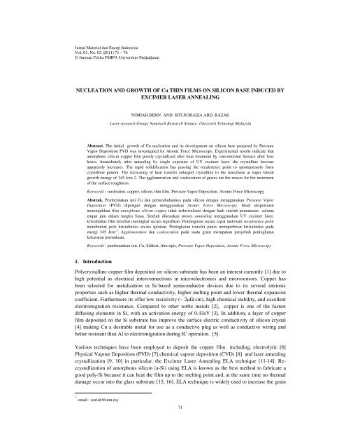
Nucleation and Growth of <strong>Cu</strong> Thin Films on Silicon base Induced by Excimer Laser Annealing 733350.0 Torr. The laser capacitor voltage was kept constant at 12 kV. The laser was externallytriggered via a AFG310 function generator to control the number of pulses bellow 10 pulses. Thedimension of laser beam spot was 2 × 4 mm 2 . The a-Si films was exposed with different number ofpulses, n. Finally, nanostructure of the crystallized silicon was examined by AFM. Figure 1 showsthe schematic diagram of the experimental setup.3. Results and DiscussionThe nucleation and the growth of SI<strong>Cu</strong> thin film was observed via AFM. The typical ofobservation results are shown in Figure 2. The Si<strong>Cu</strong> crystallization are arranged in the increasingorder of the film crystallization. Prior annealing, the grain size of the amorphous silicon thin filmwas measured. The average nanocrystal size, G av of the a-Si film before doping and heating asshown in Figure 2(a) was measured to be approximately 17 nm. After experienced four hours withconventional annealing, the nucleation of crystal was observed to form new nanostructure. Thecrystallization pattern formation almost uniform with an increment of nanocrystal size up to 56nm as depicted in frame (b) of Figure 2.Immediately after exposed by a single shot of excimer laser, with corresponding energy density of65.50 mJcm -2 , the crystal growth was observed having new pattern nanostructure. Thecrystallization of the Si<strong>Cu</strong> film was accelerated to be 75 nm as illustrated in Figure 2(c). Thecrystallization of Si<strong>Cu</strong> film was observed continuously increasing after received the sequentialnumber of pulses from excimer laser.The maximum crystallization of Si<strong>Cu</strong> film occurs after received five number of pulses as depictedin Figure 2(g). The enlargement achieved approximately as 143 nm corresponding to the fluenceof 345 mJcm -2 . Beyond this critical energy for example after treatment with six number of pulseswhich corresponding to total energy density of 389 mJcm -2 , the crystallization reduced drasticallyas illustrated in Figure 2(h). Further decreasing was observed with higher number of pulses. Thesummarization profile of nucleation and the growth of Si<strong>Cu</strong> crystal is presented in Figure 3.The surface roughness due to the melted Si<strong>Cu</strong> thin film is an alternative parameter to indicate theintergration of crystalization formation. It is used to quantify the stress develop duringsolidification. The example of surface roughness measurement is shown in Figure 4. It comprisedthe agglomeration and coalesence of grain that cause even greater surface roughness especially athigher laser fluence. Consequently the surface roughness is increasing but not beyond the SLGlimit. The maximum surface roughness was obtained as 3 nm.In general the excimer laser was partially crystallize the Si<strong>Cu</strong> film at low energy density or at lownumber of exposure. As the energy density increases the film was totally melting and freezing.The UV light of excimer laser with temperature of 6.42 eV or equivalent with 7.5 × 10 4 K wasused to melt the film and activate the <strong>Cu</strong> to diffuse into silicon base. Considering the temporallength of pulse duration each of laser pulse was only 10 ns, this means the Si<strong>Cu</strong> film wasexperience ultra-speed heating and freezing. The energetic excimer can melted higher than adecalesence point. Consequently during rapid solidification its meet a recalesence point, wherebyspontaneous pattern formation occurs and begins crystallization. The higher the heat transferredinto the Si<strong>Cu</strong> film the greater the crystallization formation. But if the delivered energy greater thansuper lateral growth of the Si<strong>Cu</strong> film, the solidification occurs before meet the recalesence point,as a result no spontaneous pattern formation consequently no crystallization. Thenanocrystallization formation indicates the solidification form in an homogenous pattern.
74 Noriah Bidin And Siti Noraiza Abd. RazakFigure 2. AFM images of Si<strong>Cu</strong> thin film with magnification area of 1000 nm x 1000 nm of (a)silicon base and (b) silicon thin film after heat treatment, and poly-Si surface after ELA with laserfluences of (c) 65.50 mJcm -2 , (d) 137.25 mJcm -2 , (e) 206.16 mJcm -2 , (f) 264.38 mJ cm -2 , (g)345.00 mJ cm -2 , (h) 389.63 mJ cm -2 , and (i) 444.75 mJ cm -2 .Figure 3. Grain size as function of number of exposureAt slow rates of crystal growth (after conventional annealing), the interface between melt and solidremains planar, and growth occurs uniformly across the surface. At faster rates of crystal growth(excimer laser annealing), instabilities are occur; this leads to crystal growth. Solidification
Nucleation and Growth of <strong>Cu</strong> Thin Films on Silicon base Induced by Excimer Laser Annealing 75releases excess energy in the form of heat at the interface between solid and melt. At slow growthrates, the heat leaves the surface by diffusion. Rapid growth creates more heat, which is dissipatedby convection (liquid flow) when diffusion is too slow. Convection breaks the planar symmetry sothat crystal growth develops along columns. The 3D micrograph of AFM in Figure 2 have clearlyshown the nucleation and the growth of Si<strong>Cu</strong> crystallization. Such nanostructure play an enormousrole in the metallization material which is beyond our scope to discuss in further detail.Figure 4. Surface roughness of Silicon Copper thin film a). after conventional heat treatment,b). single shot excimer laser annealing4. ConclusionThe nucleation and the growth of the Si<strong>Cu</strong> crystallization was observed via atomic forcemicroscope. The transformation temperature of the excimer laser capable to melt the film higherthan decalesence point. As a results, the freezing meet the recalesence point which responsible tobegin spontaneous pattern formation. The crystallization was found varies with energy density.The maximum one is met at super lateral growth energy of 345 mJcm -2 . Beyond the critical energy,the solidification occur before meeting the recalesence point which result homogenousnanostructure formation.AcknowledgementThis work has been supported from the government of Malaysia via FRGS grant vote 4F001. Wewould like to acknowledge the support given by UTM through RMC for the performance and thefinancial management of this project.
76 Noriah Bidin And Siti Noraiza Abd. RazakReferences1. K. Ma, J.Y. Feng, J. Cryst. Growth 270 (2004), 15-20.2. M.D. Thouless, Thin Solid Films 181 (1989), 397-406.3. D.K. Sarkar, S. Bera, S.V. Narasimhan, S. Chowdhury, A. Gupta, K.G.M. Nair, Solid StateCommun. 107 (1998), 413-416.4. M.Yu, J. Zhang , D. Li, Q. Meng , W. Li, Surface & Coatings Technology 201 (2006), 1243-12495. S.M. Lee, V. Zubkov, Z. <strong>Cu</strong>i, M. Shek, L.Q. Xia and H.M. Saad, Paten, US 7718548 B2, May18, 2010.6. J. Ye, Q. Chen, Y. Xiong, Y. Chai, and P. Chen. Phys. Stat. Sol. (a) 205 (2008), 1580-1584.7. F. Loffler, Surf. Coat. Technol. 132 (2000) 222-227.8. Y. Funada, K. Awazu, H. Yasui, T. Sugita, Surf. Coat. Technol. 128-129 (2000), 308-312.9. A. Gat, L.Gerzberg, J.F. Gibbons, T.J. Magee, J.Peng and J.D. Hong, Appl. Phys. Lett. 33(1978), 775-778.10. T. Serikawa, S. Shirai, A. Okamoto and S. Suyama, IEEE Trans. Electron Devices 36 (1989),1929-1933.11. T. Sameshima, S. Usui and M.Sekiya, IEEE Electron Device Lett. 7 (1986), 276-278.12. T. Sameshima, M.Hara and S. Usui, Jpn. J. Appl. Phys. 28 (1989), 1789-1793.13. R.Z. Bachrach, K. Winer, J.b. Boyce, S.E Ready, R.I. Johanson and G.B. Anderson, J. Electron.Mater. 19(1990), 241-248.14. S.N Razak, N. Bidin, Proc 2010 International Conference on Enabling Science andNanotechnology, EsciNano 2010. (Scopus).15. R. Carluccio, S. Cina, G. Fortunato, S. Friligkos, and J. Stoemenos, Thin Solid Films 296(1997), 57-60.16. M. Matsumura and C. H. Oh. Thin Solid Films 337 (1999), 123-128.17. I. A. Palani, N. J. Vasa, and M. Singaperumal, Materials Science In Semiconductor Processing11 (2008), 107-116.18. H. Watanabe, H.Miki, S. Sugai, K.Kawasaki, and T. Kioka. Jpn. J. Appl. Phys. 33 (1994),4491-4498.19. K. Brendel, N. H. Nickel, P. Lengsfeld, A. Schöpke, I. Sieber, M. Nerding, H. P. Strunk andW. Fuhs, Thin Solid Films, 427 (2003), 86-90.20. L. Mariucci, A. Pecora, G. Fortunato, C. Spinella and C. Bongiorno, Thin Solid Films 427(2003), 91-95.21. N. Bidin and S.N.Razak, Proc. Saudi Int. Electronic, Communication and Photonic Conference(SIECPC-2011), Riyadh Saudi Arabia, 24-26 April, 201122. J. Armengol, F. Vega, N. Chaoui, J. Solis, C. N. Afonso, J. Applied Physics , 93 (2003),1505-1510.23. X. Zhang and A. Atrens, Materials Science and Engineering: A, 159 (1992), 243-251.