NUCLEATION AND GROWTH OF Cu THIN FILMS ON SILICON ...
NUCLEATION AND GROWTH OF Cu THIN FILMS ON SILICON ...
NUCLEATION AND GROWTH OF Cu THIN FILMS ON SILICON ...
- No tags were found...

You also want an ePaper? Increase the reach of your titles
YUMPU automatically turns print PDFs into web optimized ePapers that Google loves.
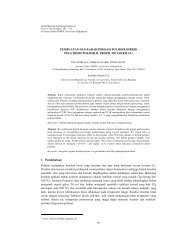
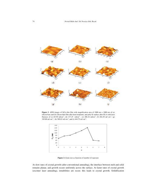
74 Noriah Bidin And Siti Noraiza Abd. RazakFigure 2. AFM images of Si<strong>Cu</strong> thin film with magnification area of 1000 nm x 1000 nm of (a)silicon base and (b) silicon thin film after heat treatment, and poly-Si surface after ELA with laserfluences of (c) 65.50 mJcm -2 , (d) 137.25 mJcm -2 , (e) 206.16 mJcm -2 , (f) 264.38 mJ cm -2 , (g)345.00 mJ cm -2 , (h) 389.63 mJ cm -2 , and (i) 444.75 mJ cm -2 .Figure 3. Grain size as function of number of exposureAt slow rates of crystal growth (after conventional annealing), the interface between melt and solidremains planar, and growth occurs uniformly across the surface. At faster rates of crystal growth(excimer laser annealing), instabilities are occur; this leads to crystal growth. Solidification