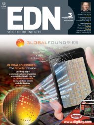
VOICE OF THE ENGINEER - ElectronicsAndBooks
VOICE OF THE ENGINEER - ElectronicsAndBooks
VOICE OF THE ENGINEER - ElectronicsAndBooks
- No tags were found...

Create successful ePaper yourself
Turn your PDF publications into a flip-book with our unique Google optimized e-Paper software.
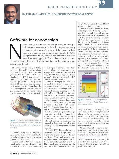
INSIDE NANOTECHNOLOGYBY PALLAB CHATTERJEE, CONTRIBUTING TECHNICAL EDITORSoftware for nanodesignNanotechnology is a diverse area that primarily involves specialty-materialproperties and effects that are prominent onlyat nanoscale dimensions. The focus of the designs in theseareas is as diverse as the materials. As a result, the CAD(computer-aided-design)-software community has not comeup with a unified approach. The market has instead chosento apply generalized mathematical and materials-based software programsto help with the task.The mathematical tools, includingWolfram Research’s (www.wolfram.com) Mathematica, The MathWorks’(www.mathworks.com) Matlab andSimulink, and PTC’s (www.ptc.com)MathCAD, determine the materials’empirical properties and the particles’actions. These general-purpose mathematicsolvers have for decades been themainstays of physics, chemistry, and engineeringgroups as the primary methodsfor addressing new technologiesFigure 1 Comsol’s Multiphysics tool letsyou model interaction analysis, such asairflow, independently of geometries fora device.and techniques by solving the primarilynonlinear or piecewise-linear fundamentalequations governing the designor molecular dynamics.Physics-based CAD and computationaltools, targeting advanced visualization,show the typical results forspecific types of analysis. These toolsinclude Comsol’s (www.comsol.com)Multiphysics, Silvaco’s (www.silvaco.com) TCAD (technology-CAD), andVerseon’s (www.verseon.com) DDA(drug-design automation).Comsol’s Multiphysics dominatesthe market due to its specialized computationalengines and ability to interactwith most 3-D-design tools andwith mathematical-modeling products,such as Matlab. Multiphysics has modulesfor ac/dc, RF, MEMS (microelectromechanicalsystems), plasma, structuralmechanics, acoustics, heat transfer,chemical-reaction engineering,batteries and fuel cells, earth science,and CFD (computational fluid dynamics).You can model interaction analysis,such as airflow, independently of geometriesfor the devices (Figure 1). Itis an equation-based tool set, so, if youuse the proper information for nanoscaleand microscopic structures, youcan analyze them in an equivalent wayto how you would analyze macroscopicstructures.Specialized TCAD tools allow you tocreate and model virtual processes andto characterize devices. Figure 2 showsthe Silvaco TCAD tool’s organic modelingof OLED (organic light-emittingdiode)displays for a photon excitation.These single-particle events are thekeys to the development of nanotechnologystructures, and they are difficultto reproduce in a laboratory.Pharmaceutical and biomedical nanotechnologyis now focusing on moleculardynamics and chemical reactionsthat form the basis of the medicationanddrug-creation industry. Verseon’sDDA product blazes a trail for a newdirection in the dynamic simulation ofdrugs. It allows for the virtual creation,simulation of interaction, and quantitativeanalysis of the combination ofknown molecules into new structures.The traditional method involves processingthe molecules into structures,separating the elements of interest,growing sufficient quantities of theseelements for testing, and then performinglaboratory-grade analysis to seethe elements’ interaction with otherFigure 2 Silvaco’s TCAD tool performsorganic modeling of OLED displays fora photon excitation.compounds. Computers simplify thesetasks, dramatically reducing the time ittakes to perform them, and allow engineersto analyze the sensitivities to singleor low numbers of interacting particles.This capability also reduces wastedtime on synthesis paths that show unpromisingresults.At the nanoscale, computer-simulationaspects are essential due to thelack of granularity and access to the devicesavailable in the macroscale.EDNPallab Chatterjee is vice chairman of theIEEE San Francisco Bay Area NanotechnologyCouncil. You can reach him atpallabc@siliconmap.net.22 EDN | SEPTEMBER 9, 2010


![[270].pdf 37407KB Sep 02 2010 09:55:57 AM - ElectronicsAndBooks](https://img.yumpu.com/50350834/1/185x260/270pdf-37407kb-sep-02-2010-095557-am-electronicsandbooks.jpg?quality=85)
![draaien, A Viruly 1935 OCR c20130324 [320]. - ElectronicsAndBooks](https://img.yumpu.com/49957773/1/190x252/draaien-a-viruly-1935-ocr-c20130324-320-electronicsandbooks.jpg?quality=85)


![20051110 c20051031 [105].pdf 35001KB Feb 18 2009 08:46:32 PM](https://img.yumpu.com/48687202/1/190x253/20051110-c20051031-105pdf-35001kb-feb-18-2009-084632-pm.jpg?quality=85)