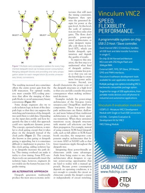
tion of energy once you factor in theirextended active time.Consider a hypothetical cellularphonedesign. Under typical usage, thecellular phone is mostly in standby mode.During standby, most circuits, except thewireless receiver or receivers, are off. Althoughstandby mode consumes onlya fraction of the power that the othermodes consume, it still consumes 36%of the total energy, after factoring in theactive period. In other words, it pays dividendsto aggressively reduce power forcircuits that are active in the standbymode because it can lead to significantsavings in battery life (Table 1).Such opportunities for energy reductionexist in most SOCs. In general, ifthe chip has multiple power domains, ithas multiple power modes. If you identifythe power modes that are most active,you can isolate the circuits thathave higher impact on the chip’s energyconsumption, and you can moreaggressively pursue power reduction inthese focused areas to reduce the overallenergy footprint of the chip.Analysis of these circuits in furtherdetail uncovers some interesting characteristics.These modules must remainon for extended periods because theyperform essential functions for the chipin that operating mode. They are oftencontinuously calculating data or processingsignals. In addition to the cellular-phoneexample, other circuits, suchas audio or video processors in playbackor talk mode and signal-processingblocks, such as equalizer, modulation,or cryptology units, in wireless and networkingapplications, have more datapathcontent than control logic andcan benefit considerably from low-powertechniques.If you consider the technology horizon,a new generation of connected devicesaiming to deliver better user experiencesand higher data rates is drivingmany new design starts. Consequently,these new projects will demand higherAT A GLANCE↘ Design engineers are increasinglyemploying advanced techniquesto meet the more stringent powerrequirements of next-generationchips.↘ It pays dividends to aggressivelyreduce power for circuits that areactive in standby mode because itcan lead to significant savings inbattery life.↘ Power gating isn’t feasible forcircuits that must continuouslyremain active, so the only choice isto make the circuit intrinsically lowpower.↘ Traditionally, datapath generatorsproduce the most area-economicarchitectures that still meet the timingconstraints.↘ Because power is a physicaldomaincharacteristic, your standardcelllibrary can affect the power-optimizationresult.audio quality, higher video resolution,more pixel support, more complex signalprocessing, faster data rates, and soforth. Increases in the size and complexityof the signal-processing blocksin turn lead to a higher energy footprintin the new designs. The impact of thisdesign complexity requires design engineersto more closely manage the powerconsumption for these blocks.LOW-POWER DATAPATHSPower gating isn’t feasible for circuitsthat must continuously remain active,so the only choice is to make the circuitintrinsically low power. The firststep is to lower the voltage, the operatingfrequency, or both without missingthe performance target. However,slower clock frequencies mean deeperlogic levels, and these circuits usuallyinclude more datapath logic than controllogic. Datapath logic is notoriouslyTABLE 1 SAMPLE POWER MODES AND ENERGY CONSUMPTIONPower modePower consumption(mW)Time budgetedin mode (%)Energy-consumptionprofileStandby 40 90 36Audio 400 3 12Phone 500 5 25Video 1200 2 24prone to glitches—unwanted transitionsthat settle before the next clockedge—and switching because any spurioustransitions propagate downstreamand ripple throughout the entire datapathtree. Although glitches pose nofunctional issues, these transitions stillconsume power.It is critical to avoid increasing powerin other areas while reducing it in onearea. Making this power-reduction approachmore effective requires more balanced,shallower architectures that canlimit the propagation of the transitions.Although most EDA tools do an adequatejob producing timing- and areaoptimizedarchitectures that designerslater optimize for power at the gate level,they are less effective in consideringthe power consequence of architecturalselections upfront.Some design engineers try variousmeans of writing power-optimized architecturesinto RTL (register-transfer-level)code to save power. However, mostlow-power architectural-RTL coding focuseson reducing area, based on the assumptionthat using fewer cells equatesto less power consumption. For example,some design engineers in networkingand multimedia applications truncatethe LSBs (least-significant bits) of thedata when precision is not critical.Although this technique is useful,you must understand the details of howto implement it. Datapaths differ fromother logic circuits in that they performcomputer arithmetic that generatescarries and sums, requiring carry-propagatingadders to add together the carryand sum to produce a binary number.For RTL coded at a high level, EDAtools usually can generate datapath architectures,keeping all the numbers inredundant format—annotating the valueof the number with both carry andsum—until the last level of the output.If you code the datapath at a lowerlevel, you might turn to coding practicesthat divide a larger datapath block intoseveral small ones,forcing the RTLsynthesistools toinsert carry-propagationadders intothe final stageof every smallerblock (Figure 1a),hence increasingarea and delay.26 EDN | SEPTEMBER 9, 2010
SELECTA(a)BSELECTThe resulting increased area sometimesoffsets the entire power gain from theLSB truncation. For optimal results,you must consider RTL-coding practicesthat allow the merging of datapathblocks to avoid unnecessary binaryconversions (Figure 1b).Some design engineers also try tocode isolation logic in front of the datapathlogic so that they can suppress theswitching and transition of the datapathtree until there is valid data. Dependingon the input-data profile and how frequentlythe data is valid, this approachcould save significant dynamic power.The concept, operand isolation, is similarto clock gating, except that it takesplace on the datapath instead of theclock paths (Figure 2). The concept,also known as data gating or datapathgating, is appealing, but it is sometimesdifficult to implement in practice. Unlikeclock gating, adding isolation logicto datapaths increases the path delay.This timing overhead can make ittricky to close timing. Some RTL-synthesistools can automatically insert theisolation logic; however, engineers donot widely use the feature because it degradestiming.E0 0Figure 1 Multiple carry-propagation adders for every fragmenteddatapath block (a) increase power consumption.Merging datapath blocks and providing one carry-propagationadder for each merged block (b) avoids unnecessarybinary conversions.A(b)B+EAN ALTERNATIVE APPROACHDatapath generators traditionallyproduce the most area-economic architecturesthat still meetthe timing constraints.Engineers then optimizethe generated designsfor power at thegate level. At this level,the scale of optimizationinvolves only a fewgates. The flows don’tprovide power-optimizedarchitectures, sosome designers manuallycode them in lowlevelRTL, which canhinder datapath optimizationand degradethe quality of results.To improve this situation,the first step is tounderstand what kindof datapath architecturesconsume less powerso that you can usethe knowledge to createmore low-power architectures.Second, youshould characterize the power costs ofthe datapath structures at a high levelso that you can fully consider the powerconsequences when making architecturaldecisions.Examples include the power-stingyarchitectures of the Synopsys (www.synopsys.com) DesignWare minPowercomponents. These low-power datapatharchitectures are flatter, shallower,and more balanced than traditionalarchitectures to produce fewer spurioustransitions. When these unwantedtransitions occur, datapath structureswith smarter cell selections can limittheir propagation. For example, insteadof using common XOR-based datapathcells, such as full adders or XOR-basedbooth encoders, the manpower componentsemploy architectures that favormore AND or NAND cells so thatfewer transitions ripple throughout thedatapath tree.Integrating these power-friendly architecturesyields some advantages.Aside from being easier to use, thesearchitectures allow designers to capturepower-saving opportunities thatare hard to realize with a manual approach.Because power consumptiondepends on operating conditions, it isnot enough to consider the circuit architectureoutside the design’s contextor independently of circuit switching.Vinculum VNC2SPEED.FLEXIBILITY.PERFORMANCE.A programmable system-on-chipUSB 2.0 Host / Slave controller.- Dual channel USB 2.0 interface, handlesall USB host and data transfer functionsin single IC.- On-chip 16-bit Harvard architectureMCU core with 256 Kbyte Flash and16kbyte RAM.- External UART, FIFO, SPI Slave, SPI Master,GPIO and PWM interfaces.- Vinculum-II software development toolsavailable for user application development.- Multiple package size options including VNC1Lbackwards compatible package option.- Targeted for range of USB applications, fromportable media devices and cell phones toindustrial and automotive applications.Vinculum-II evaluation modules- V2DIP1/2 - Miniature VNC2 DevelopmentModule with Single or Dual USB Connectors- V2-EVAL - Complete Evaluation &Development Kit for VNC2- VNC2 Debug ModuleUSB MADE EASYwww.ftdichip.com


![[270].pdf 37407KB Sep 02 2010 09:55:57 AM - ElectronicsAndBooks](https://img.yumpu.com/50350834/1/185x260/270pdf-37407kb-sep-02-2010-095557-am-electronicsandbooks.jpg?quality=85)
![draaien, A Viruly 1935 OCR c20130324 [320]. - ElectronicsAndBooks](https://img.yumpu.com/49957773/1/190x252/draaien-a-viruly-1935-ocr-c20130324-320-electronicsandbooks.jpg?quality=85)


![20051110 c20051031 [105].pdf 35001KB Feb 18 2009 08:46:32 PM](https://img.yumpu.com/48687202/1/190x253/20051110-c20051031-105pdf-35001kb-feb-18-2009-084632-pm.jpg?quality=85)