VOICE OF THE ENGINEER - ElectronicsAndBooks
VOICE OF THE ENGINEER - ElectronicsAndBooks
VOICE OF THE ENGINEER - ElectronicsAndBooks
- No tags were found...

You also want an ePaper? Increase the reach of your titles
YUMPU automatically turns print PDFs into web optimized ePapers that Google loves.
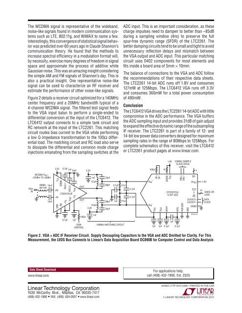
The WCDMA signal is representative of the wideband,noise-like signals found in modern communication systemssuch as LTE, 802.11g, and WiMAX to name a few.Interestingly, this convergence of statistical signal behaviorwas predicted over 60 years ago in Claude Shannon’scommunication theory. He found that the methods toincrease spectral effi ciency in a modulation format will,by necessity, exercise many degrees of freedom in signalspace and approximate the process of additive whiteGaussian noise. This was an amazing insight consideringthe simple AM and FM signals of Shannon’s day. This isalso a practical insight. One representative noise-likesignal can be used to characterize an RF receiver andestimate the performance of other noise-like signals.Figure 2 details a receiver circuit optimized for a 140MHzcenter frequency and a 20MHz bandwidth typical of a4-channel WCDMA signal. The fi ltered test signal feedsto the VGA input balun to perform a single-ended todifferential conversion at the input of the LTC6412. TheLTC6412 output connects to a simple tank circuit andRC network at the input of the LTC2261. This matchingcircuit routes bias current to the VGA while performinga low Q impedance transformation to the 100Ω differentialload. The matching circuit and RC load also serveto dissipate the differential and common mode chargeinjections emanating from the sampling switches at theADC input. This is an important consideration, as thesecharge impulses need to dampen to better than –85dBduring a sampling window (4ns) to preserve the fullspur-free dynamic range (SFDR) of the LTC2261. Thebetter damping circuits tend to be small and tight to avoidunnecessary refl ection delays and mismatch betweenthe VGA output and ADC input. This particular matchingcircuit uses 0402 components for most elements andfi ts inside a board area of 5mm × 10mm.The balance of connections to the VGA and ADC followthe recommendations of their respective data sheets.The LTC2261 14-bit ADC runs off 1.8V and consumes127mW at 125Msps. The LTC6412 VGA runs off 3.3Vand consumes 360mW for a total power consumptionof 490mW.ConclusionThe LTC6412 VGA drives the LTC2261 14-bit ADC with littlecompromise in the ADC performance. The VGA buffersthe ADC sampling input and provides 31dB of gain adjustto expand the effective dynamic range of the subsamplingIF receiver. The LTC2261 is part of a family of 12- and14-bit low power data converters designed for maximumsampling rates in the range of 80Msps to 125Msps. Forcomplete schematics of this receiver, visit the LTC6412or LTC2261 product pages at www.linear.com.1.8V125MHz SAMPLECLOCK DRIVE3.3V0.1μF 1nF 10nF 3.3V100Ω1k450ΩINWCDMA P IN =–22dBm TO +9dBm••MABA-00715910nF10nFVCC+IN–INGNDENSHDNDECL1DECL2LTC6412CUF+V GVREF–VGV CM+OUT–OUT1nF47μH47μH3.3V22pF68pF 0.1μF 51Ω68pF 1nF 51Ω22pF4.7pF4.7pFA IN+A IN–VCM0F+<strong>OF</strong>–VREFVDDSENSELTC2261CUJ14-BIT ADCREFHREFLENC+ENC–PAR/SERGNDSPIOV DDD13 • •D0CLKOUT+CLKOUT–OGND141.8VCMOS ORLVDSDATACLOCK0.1μF1μF100ΩGAINCONTROL1nF140MHz MATCHING CIRCUIT1μF1μF0.1μF1μF0.1μFDN4WS F02Figure 2. VGA + ADC IF Receiver Circuit. Supply Decoupling Capacitors to the VGA and ADC Omitted for Clarity. For ThisMeasurement, the LVDS Bus Connects to Linear’s Data Acquisition Board DC890B for Computer Control and Data AnalysisData Sheet Downloadwww.linear.comFor applications help,call (408) 432-1900, Ext. 2525Linear Technology Corporation1630 McCarthy Blvd., Milpitas, CA 95035-7417(408) 432-1900 FAX: (408) 434-0507 www.linear.comdn482f LT/TP 0910 226K • PRINTED IN <strong>THE</strong> USA© LINEAR TECHNOLOGY CORPORATION 2010


![[270].pdf 37407KB Sep 02 2010 09:55:57 AM - ElectronicsAndBooks](https://img.yumpu.com/50350834/1/185x260/270pdf-37407kb-sep-02-2010-095557-am-electronicsandbooks.jpg?quality=85)
![draaien, A Viruly 1935 OCR c20130324 [320]. - ElectronicsAndBooks](https://img.yumpu.com/49957773/1/190x252/draaien-a-viruly-1935-ocr-c20130324-320-electronicsandbooks.jpg?quality=85)


![20051110 c20051031 [105].pdf 35001KB Feb 18 2009 08:46:32 PM](https://img.yumpu.com/48687202/1/190x253/20051110-c20051031-105pdf-35001kb-feb-18-2009-084632-pm.jpg?quality=85)