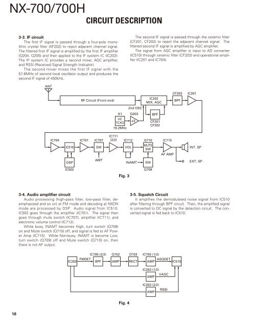
<strong>NX</strong>-<strong>700</strong>/<strong>700</strong>HCIRCUIT DESCRIPTION3-3. IF circuitThe first IF signal is passed through a four-pole monolithiccrystal filter (XF202) to reject adjacent channel signal.The filtered first IF signal is amplified by the first IF amplifier(Q204, Q205) and then applied to the lF system IC (IC202).The IF system IC provides a second mixer, AGC amplifier,and RSSI (Received Signal Strength Indicator).The second mixer mixes the first IF signal with the57.6MHz of second local oscillator output and produces thesecond IF signal of 450kHz.The second IF signal is passed through the ceramic filter(CF201, CF202) to reject the adjacent channel signal. Thefiltered second IF signal is amplified by AGC amplifier.The signal from AGC amplifier is input to AD converter(IC510) through ceramic filter (CF203) and operational amplifier(IC201 and IC704).ANTRF Circuit (Front end)IC202MIX. AGCCF203BPFIC2012nd OSCX1VCTCXO19.2MHzQ203x3BPFCF201CF202IC704IC510IC701IC707SWIC711(2/2)IC712VOLQ710MUTESWIC715AF AMPINT. SPDSPAMTINAMTSWEXT. SPIC502Q709Fig. 33-4. Audio amplifier circuitAudio processing (high-pass filter, low-pass filter, deemphasizedand so on) at FM mode and decoding at <strong>NX</strong>DNmode are processed by DSP. Audio signal from IC510,IC502 goes through the amplifier (IC701). The signal thengoes through mute switch (IC707), amplifier (IC711), andelectronic volume control (IC712).While busy, INAMT becomes High, turn switch (Q709)on and Mute switch (Q710) off, and signal is fed to AF PowerAmp (IC715). While Non-busy, INAMT is become Low,turn switch (Q709) off and Mute switch (Q710) on, thenthere is not AF output.3-5. Squelch CircuitIt amplifies the demodulated noise signal from IC510after filtering through BPF circuit. Then, the amplified signalis converted to DC signal by the detection circuit. The convertedsignal is fed back to IC510.IC202IC705 (2/2)FMDETBPFQ702AMPD703RECTIC705 (1/2)ASQDETAMPIC510IC203 (1/2)VAGCAMPIC203 (2/2)RSSIAMPFig. 418
CIRCUIT DESCRIPTION<strong>NX</strong>-<strong>700</strong>/<strong>700</strong>H4. Transmitter System4-1. Audio Band CircuitThe signal from the microphone goes through the muteswitch (Q706), the Mic-Mute signal (MM) becomes Low,then mute switch (Q706) is turned off. The signal frommicrophone goes through Mic-AGC (Q704, Q705, D704,D705), and goes through switch IC (IC708), and amplified byMic-Amp IC706 (1/2), LPF IC706 (2/2) works as anti-aliasingfilter.If an optional scrambler board is installed, the switch(IC708) adjusts the signal path so that the audio signal is inputto the scrambler board.INT. MICQ707Optional Scrambler BoardD703,D704Q705,Q706IC7084-2. Base Band CircuitThe audio signal output from the base band circuit isconverted to digital data of a sampling frequency of 48kHz.This digital data is sent to the DSP (IC502), and voice signalsof 300Hz or lower and frequencies of 3kHz or higher arecut off and an audio range 300Hz to 3kHz is extracted. Theaudio signal is then pre-emphasized in FM mode and synthesizedwith the signals, such as QT and DQT, as required,and is then output from the IC510. In Digital mode, the audiosignal is converted to the 4-Level FSK base band signaland output from the IC510. The DTMF and MSK base bandsignals are also generated by the DSP and output by theIC510.LPF (IC702) works as smoothing filter. The DAC (IC712)assigns the base band signal to the VCO and VCTCXO (X1).At this time, the level output according to the transmit carrieris fine-adjusted according to each modulation method.IC706(1/2)IC706(1/2)IC502DSPSWAGCSWAMPLPFIC510MMSCSWIC1X1LPFLPFAMPIC712AMPVCTCXOIC702(2/2)IC702(1/2)IC709(1/2)AMPVCOFig. 5IC5 (2/2)4-3. Drive and Final amplifierThe transmit signal obtained from the TX VCO bufferamplifier Q9, is amplified to approximately +17dBm by thedriver amplifiers Q14, Q101 and Q102.This amplified signal is passed to the power amplifiermodule (power module) IC102, which consists of a MOS-FET amplifier and capable of transmission output power.4-4. APC circuitThe Automatic transmission power control (APC) circuitstabilizers the transmitter output power at a predeterminedlevel by detecting the power module output with a diodesD107, D108 and D109. Diodes D107, D108 and D109 applya voltage to DC amplifier IC103 (1/2).IC103 (2/2) compares the APC control voltage (PC) generatedby microprocessor IC510 and DC amplifier IC101 (1/2,2/2) with the detection output voltage from IC103 (1/2) tocontrol the Vgg Pin of IC102, and stabilizes transmission output.The APC circuit is configured to protect over-current ofthe power module due to fluctuations of the load at theantenna end and to stabilize transmission output at voltageand temperature variations.Buff AMPQ13Drive AMPQ140dBmDrive AMPQ101Drive AMPQ102+17dBmFinal AMPIC102*D103: <strong>NX</strong>-<strong>700</strong>H onlyD103*,D104,D105,D215ANTMODTX VCOSWANT FilterMBVCTCXO19.2MHzPCMPDCAMPIC101GatebiasDCAMPIC103D107 D108 D109DET DET DETFig. 619