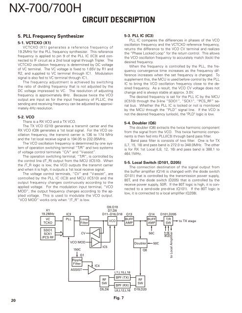
<strong>NX</strong>-<strong>700</strong>/<strong>700</strong>HCIRCUIT DESCRIPTION5. PLL Frequency Synthesizer5-1. VCTCXO (X1)VCTCXO (X1) generates a reference frequency of19.2MHz for the PLL frequency synthesizer. This referencefrequency is applied to pin 9 of the PLL IC (IC3) and connectedto IF circuit as a 2nd local signal through Tripler. TheVCTCXO oscillation frequency is determined by DC voltageof VC terminal. The VC voltage is fixed to 1.65V by R1 andR2, and supplied to VC terminal through IC1. Modulationsignal is also fed to VC terminal through IC1.The frequency adjustment is achieved by switchingthe ratio of dividing frequency that is not adjusted by theDC voltage impressed to VC. The resolution of adjustingfrequency is approximately 8Hz. Because twice the VCOoutput are input as for the input frequency of PLLIC, thesending and receiving frequency can be adjusted by approximately4Hz resolution.5-2. VCOThere is a RX VCO and a TX VCO.The TX VCO (Q10) generates a transmit carrier and theRX VCO (Q9) generates a 1st local signal. For the VCO oscillationfrequency, the transmit carrier is 136 to 174 MHzand the 1st local receive signal is 194.05 to 232.05MHz.The VCO oscillation frequency is determined by one systemof operation switching terminal “T/R” and two systemsof voltage control terminals “C/V” and “V-assist”.The operation switching terminal, “T/R”, is controlled bythe control line (/T_R) output from the MCU (IC510). Whenthe /T_R logic is low, the VCO outputs the transmit carrierand when it is high, it outputs a 1st local receive signal.The voltage control terminals, “CV” and “V-assist”, arecontrolled by the PLL IC (IC3) and MCU (IC510) and theoutput frequency changes continuously according to theapplied voltage. For the modulation input terminal, “VCOMOD”, the output frequency changes according to the appliedvoltage. This is used to modulate the VCO output.“VCO MOD” works only when “/T_R” is low.5-3. PLL IC (IC3)PLL IC compares the differences in phases of the VCOoscillation frequency and the VCTCXO reference frequency,returns the difference to the VCO CV terminal and realizesthe “Phase Locked Loop” for the return control. This allowsthe VCO oscillation frequency to accurately match (lock) thedesired frequency.When the frequency is controlled by the PLL, the frequencyconvergence time increases as the frequency differenceincreases when the set frequency is changed. Tosupplement this, the MCU is used before control by the PLLIC to bring the VCO oscillation frequency close to the desiredfrequency. As a result, the VCO CV voltage does notchange and is always stable at approx. 3.0V.The desired frequency is set for the PLL IC by the MCU(IC510) through the 3-line “SDO1”, “SCK1”, “PCS_RF” serialbus. Whether the PLL IC is locked or not is monitoredby the MCU through the “PLD” signal line. If the VCO isnot the desired frequency (unlock), the "PLD" logic is low.5-4. Doubler (Q6)The doubler (Q6) extracts the twice harmonic componentfrom the signal from the VCO. This twice harmonic componentsis then fed into PLL(IC3) through band pass filter.Band pass filter is consists of two filter. One is for TX(L7, 15, 18) and pass band is 272.0 to 348.0MHz. The otheris for RX 1st Local (L8, 12, 16) and pass band is 388.1 to464.1MHz.5-5. Local Switch (D101, D205)The connection destination of the signal output fromthe buffer amplifier (Q14) is changed with the diode switch(D101) that is controlled by the transmission power supply,80T, and the diode switch (D205) that is controlled by thereceive power supply, 50R. If the 80T logic is high, it is connectedto a send-side pre-drive (Q101). If the 80T logic islow, it is connected to a local amplifier (Q208).X119.2MHzVCTCXOIC3PLLLoopFilterQ9,Q10D7,D8D11~D16,D18VCOQ13BUFFAMPQ14BUFFAMPD101,D205T/RSWto TX stageSDO1SCK1/PCS RF150CCVVCO MODQ1RippleFilterASSISTIC4IC5RFSWD5,D6L7,L15,L18BPF (TX)BPF (RX)L8,L12,L16DoublerQ6RFSWD19,D2050C50C80T50Rto Local Amplifier20Fig. 7
CIRCUIT DESCRIPTION<strong>NX</strong>-<strong>700</strong>/<strong>700</strong>H6. Control CircuitThe control circuit consists of MCU (IC510) and its peripheralcircuits. IC510 mainly performs the following;1) Switching between transmission and reception by PTTsignal input.2) Reading system, zone, frequency, and program datafrom the memory circuit.3) Sending frequency program data to the PLL.4) Controlling squelch on/off by the DC voltage from thesquelch circuit.5) Controlling the audio mute circuit by decode data input.6-1. MCUThe MCU (IC510) is 32bit RISC processor, equipped withperipheral function and ADC/DAC.This MCU operates at 18.432MHz clock and 3.3V /1.5VDC. Controls the flash memory, SRAM, DSP, the receivecircuit, the transmitter circuit, the control circuit, and the displaycircuit and transfers data to or from an external device.6-2. Memory CircuitMemory circuit consists of the MCU (IC510) and theSRAM (IC503), the flash memory (IC501). The flash memoryhas capacity of 32Mbit that contains the transceiver controlprogram for the MCU and stores the data. It also storesthe data for transceiver channels and operating parameterthat are written by the FPU. This program can be easilywritten from external devices. The SRAM has capacity of1Mbit that contains work area and data area.■ Flash memoryNote: The flash memory stores the data that is writtenby the FPU (KPG-111D), tuning data (Deviation, Squelch,etc.), and firmware program.■ SRAM (static memory)Note: The SRAM has temporary data area and workarea.When the power supply is off, it is backed up by an internalsecondary lithium battery. Therefore, the save data doesnot break.■ Real-time clockThe clock function is based on real-time clock IC (IC504).When the power supply is off, it is backed up by an internalsecondary lithium battery6-3. Display UnitThe display unit is composed of the MCU (IC911) andthe memory IC (IC913), and the LCD & Key backlight etc.The LCD Ass’y (with LCD Driver) is controlled using thebus lines on the connector (CN905) of the display unit. Itcorrects the LCD contrast voltage using IC909.6-4. Key Detection CircuitKeys are detected using Key scan circuit in IC911. The/KI* and KO* signals that are normally pulled up go lowwhen any key is pressed.6-5. DSPThe DSP circuit consists of a DSP (IC502) and processesthe base band signal. The DSP operates on an externalclock of 18.432MHz (the same as the IC510), the I/O sectionoperates at 3.3V and the core section operates at 1.5V.The DSP carries out the following processes:• 4Level FSK processing• Analog FM pre-emphasis/de-emphasis• Vocoder processing between audio codec and modulation/demodulation• CAI processing, such as error correction encoding• QT/DQT encoding/decoding• DTMF encoding/decoding• MSK encoding/decoding• 2TONE encoding/decoding• Compressor/expander processing• Voice scrambler processing• Transmit/receive audio filtering processing• Microphone amplifier AGC processing• Audio mute processing• Modulation level processing7. Power Supply Circuit+B is connected to Final amplifier and DC/DC converterIC (IC405). IC405 regulates +B voltage to 5.0V (50M). 50Moperates whenever +B is supplied. IC402 (33M), IC408 (33A)and IC409 (15M) are enabled while the 50M are operating.33M and 15M provide the power to MCU, DSP, andFlash memory. At this time MCU starts working. Voltagedetector IC (IC401) watches +B voltage. If +B voltage ishigher than 8.6V, IC401 (/BINT) outputs High. If the /BINTsignal is high, Q404 (SB SW) is turned on by SBC signalfrom MCU. (High: SB=ON, Low: SB=OFF). When the SBis turned on, IC403 (80C), IC404 (50C), IC406 (33C), IC407(33GPS) and IC410 (150C) start working. Q416 and Q412are controlled by SBC signal. If the SBC signal becomesHigh, Q416 (33A-2) operates and Q412 (50MC SW) areturned on.The MCU controls the TXC signal to High during transmissionto supply power (80T) for transmission circuit. TheMCU controls the signals (RXC) to High during reception tosupply power (80R, 50R) for reception circuit.When the MCU detects the PSW (Power switch) signal,IGN (Ignition sense) signal or /BINT signal, it controls theSBC signal to Low, and turns the transceiver power (SB) off.When D401 and Q401 detect over-voltage condition, theyturns Q404 (SB SW) off. But the MCU still works.If +B is not provided to the transceiver, the power is providedto SRAM and RTC through the secondary battery connectedwith CN405.21