High Voltage Transistors BF420 BF422 - Futurlec
High Voltage Transistors BF420 BF422 - Futurlec
High Voltage Transistors BF420 BF422 - Futurlec

Create successful ePaper yourself
Turn your PDF publications into a flip-book with our unique Google optimized e-Paper software.
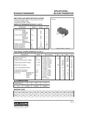
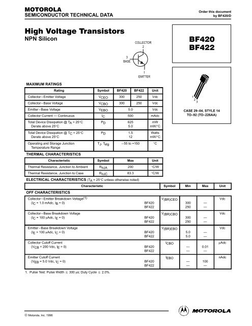
SEMICONDUCTOR TECHNICAL DATAOrder this documentby <strong>BF420</strong>/D NPN Silicon3BASECOLLECTOR21EMITTERMAXIMUM RATINGSRating Symbol <strong>BF420</strong> <strong>BF422</strong> UnitCollector–Emitter <strong>Voltage</strong> VCEO 300 250 VdcCollector–Base <strong>Voltage</strong> VCBO 300 250 VdcEmitter–Base <strong>Voltage</strong> VEBO 5.0 VdcCollector Current — Continuous IC 500 mAdcTotal Device Dissipation @ TA = 25°CDerate above 25°CPD 6255.0mWmW/°C123CASE 29–04, STYLE 14TO–92 (TO–226AA)Total Device Dissipation @ TC = 25°CDerate above 25°CPD 1.512WattsmW/°COperating and Storage JunctionTemperature RangeTJ, Tstg –55 to +150 °CTHERMAL CHARACTERISTICSCharacteristic Symbol Max UnitThermal Resistance, Junction to Ambient R JA 200 °C/WThermal Resistance, Junction to Case R JC 83.3 °C/WELECTRICAL CHARACTERISTICS (TA = 25°C unless otherwise noted)OFF CHARACTERISTICSCollector–Emitter Breakdown <strong>Voltage</strong>(1)(IC = 1.0 mAdc, IB = 0)Collector–Base Breakdown <strong>Voltage</strong>(IC = 100 Adc, IE = 0)Emitter–Base Breakdown <strong>Voltage</strong>(IE = 100 Adc, IC = 0)Collector Cutoff Current(VCB = 200 Vdc, IE = 0)Emitter Cutoff Current(VEB = 5.0 Vdc, IC = 0)1. Pulse Test: Pulse Width 300 s; Duty Cycle 2.0%.Characteristic Symbol Min Max Unit<strong>BF420</strong><strong>BF422</strong><strong>BF420</strong><strong>BF422</strong><strong>BF420</strong><strong>BF422</strong><strong>BF420</strong><strong>BF422</strong><strong>BF420</strong><strong>BF422</strong>V(BR)CEOV(BR)CBOV(BR)EBOICBOIEBO3002503002505.05.0——————————0.01—100—VdcVdcVdcµAdcnAdcMotorola Small–Signal <strong>Transistors</strong>, FETs and Diodes Device Data© Motorola, Inc. 19961
ELECTRICAL CHARACTERISTICS (TA = 25°C unless otherwise noted) (Continued)ON CHARACTERISTICSDC Current Gain(IC = 25 mAdc, VCE = 20 Vdc)Collector–Emitter Saturation <strong>Voltage</strong>(IC = 20 mAdc, IB = 2.0 mAdc)Characteristic Symbol Min Max Unit<strong>BF420</strong><strong>BF422</strong>hFEVCE(sat)5050——— 0.5—VdcBase–Emitter Saturation <strong>Voltage</strong>(IC = 20 mAdc, IB = 2.0 mAdc)VBE(sat)— 2.0VdcSMALL–SIGNAL CHARACTERISTICSCurrentGain — Bandwidth Product(IC = 10 mAdc, VCE = 10 Vdc, f = 20 MHz)fT60 —MHzCommon Emitter Feedback Capacitance(VCB = 30 Vdc, IE = 0, f = 1.0 MHz)Cre— 1.6pF2 Motorola Small–Signal <strong>Transistors</strong>, FETs and Diodes Device Data
200VCE = 10 VdchFE, DC CURRENT GAIN1005030TJ = +125°C25°C–55°C201.0 2.0 3.0 5.0 7.0 10 20 30 50 70IC, COLLECTOR CURRENT (mA)100Figure 1. DC Current GainC, CAPACITANCE (pF)1005020105.02.01.00.2CebCcb0.5 1.0 2.0 5.0 10 20 50 100 200VR, REVERSE VOLTAGE (VOLTS)f T , CURRENT–GAIN — BANDWIDTH PRODUCT (MHz)10070503020101.02.03.05.07.010TJ = 25°CVCE = 20 Vf = 20 MHz20IC, COLLECTOR CURRENT (mA)305070100Figure 2. CapacitancesFigure 3. Current–Gain — Bandwidth ProductV, VOLTAGE (VOLTS)1.41.21.00.80.60.40.201.02.0TJ = 25°CVBE(sat) @ IC/IB = 10VBE(on) @ VCE = 10 VVCE(sat) @ IC/IB = 103.0 5.0 7.0 10 20 30IC, COLLECTOR CURRENT (mA)5070100IC, COLLECTOR CURRENT (mA)500200100TA = 25°CTC = 25°C100 µs1.0 ms50100 ms2010CURRENT LIMITTHERMAL LIMIT5.0(PULSE CURVES @ TC = 25°C)SECOND BREAKDOWN LIMIT2.0CURVES APPLY1.0BELOW RATEDMPSA43VCEOMPSA420.50.5 1.0 2.0 5.0 10 20 50 100 200 500VCE, COLLECTOR–EMITTER VOLTAGE (VOLTS)10 µsFigure 4. “On” <strong>Voltage</strong>sFigure 5. Maximum Forward BiasSafe Operating AreaMotorola Small–Signal <strong>Transistors</strong>, FETs and Diodes Device Data3
PACKAGE DIMENSIONSSEATINGPLANERAX XHV1NFGPNBLKCDJSECTION X–XNOTES:1. DIMENSIONING AND TOLERANCING PER ANSIY14.5M, 1982.2. CONTROLLING DIMENSION: INCH.3. CONTOUR OF PACKAGE BEYOND DIMENSION RIS UNCONTROLLED.4. DIMENSION F APPLIES BETWEEN P AND L.DIMENSION D AND J APPLY BETWEEN L AND KMINIMUM. LEAD DIMENSION IS UNCONTROLLEDIN P AND BEYOND DIMENSION K MINIMUM.INCHES MILLIMETERSDIM MIN MAX MIN MAXA 0.175 0.205 4.45 5.20B 0.170 0.210 4.32 5.33C 0.125 0.165 3.18 4.19D 0.016 0.022 0.41 0.55F 0.016 0.019 0.41 0.48G 0.045 0.055 1.15 1.39H 0.095 0.105 2.42 2.66J 0.015 0.020 0.39 0.50K 0.500 ––– 12.70 –––L 0.250 ––– 6.35 –––N 0.080 0.105 2.04 2.66P ––– 0.100 ––– 2.54R 0.115 ––– 2.93 –––V 0.135 ––– 3.43 –––CASE 029–04(TO–226AA)ISSUE ADSTYLE 14:PIN 1. EMITTER2. COLLECTOR3. BASEMotorola reserves the right to make changes without further notice to any products herein. Motorola makes no warranty, representation or guarantee regardingthe suitability of its products for any particular purpose, nor does Motorola assume any liability arising out of the application or use of any product or circuit,and specifically disclaims any and all liability, including without limitation consequential or incidental damages. “Typical” parameters can and do vary in differentapplications. All operating parameters, including “Typicals” must be validated for each customer application by customer’s technical experts. Motorola doesnot convey any license under its patent rights nor the rights of others. Motorola products are not designed, intended, or authorized for use as components insystems intended for surgical implant into the body, or other applications intended to support or sustain life, or for any other application in which the failure ofthe Motorola product could create a situation where personal injury or death may occur. Should Buyer purchase or use Motorola products for any suchunintended or unauthorized application, Buyer shall indemnify and hold Motorola and its officers, employees, subsidiaries, affiliates, and distributors harmlessagainst all claims, costs, damages, and expenses, and reasonable attorney fees arising out of, directly or indirectly, any claim of personal injury or deathassociated with such unintended or unauthorized use, even if such claim alleges that Motorola was negligent regarding the design or manufacture of the part.Motorola and are registered trademarks of Motorola, Inc. Motorola, Inc. is an Equal Opportunity/Affirmative Action Employer.How to reach us:USA/EUROPE: Motorola Literature Distribution;JAPAN: Nippon Motorola Ltd.; Tatsumi–SPD–JLDC, Toshikatsu Otsuki,P.O. Box 20912; Phoenix, Arizona 85036. 1–800–441–2447 6F Seibu–Butsuryu–Center, 3–14–2 Tatsumi Koto–Ku, Tokyo 135, Japan. 03–3521–8315MFAX: RMFAX0@email.sps.mot.com – TOUCHTONE (602) 244–6609 HONG KONG: Motorola Semiconductors H.K. Ltd.; 8B Tai Ping Industrial Park,INTERNET: http://Design–NET.com 51 Ting Kok Road, Tai Po, N.T., Hong Kong. 852–266292984 ◊Motorola Small–Signal <strong>Transistors</strong>, FETs and Diodes Device <strong>BF420</strong>/D Data