2SJ160, 2SJ161, 2SJ162 - Jaycar Electronics
2SJ160, 2SJ161, 2SJ162 - Jaycar Electronics
2SJ160, 2SJ161, 2SJ162 - Jaycar Electronics

You also want an ePaper? Increase the reach of your titles
YUMPU automatically turns print PDFs into web optimized ePapers that Google loves.
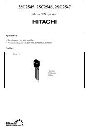
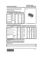
<strong>2SJ160</strong>, <strong>2SJ161</strong>, <strong>2SJ162</strong>Silicon P-Channel MOS FETApplicationLow frequency power amplifierComplementary pair with 2SK1056, 2SK1057 and 2SK1058Features• Good frequency characteristic• High speed switching• Wide area of safe operation• Enhancement-mode• Good complementary characteristics• Equipped with gate protection diodes• Suitable for audio power amplifier
123<strong>2SJ160</strong>, <strong>2SJ161</strong>, <strong>2SJ162</strong>OutlineTO-3PDGS1. Gate2. Source(Flange)3. DrainAbsolute Maximum Ratings (Ta = 25°C)Item Symbol Ratings UnitDrain to source voltage <strong>2SJ160</strong> V DSX –120 V<strong>2SJ161</strong> –140<strong>2SJ162</strong> –160Gate to source voltage V GSS ±15 VDrain current I D –7 ABody to drain diode reverse drain current I DR –7 AChannel dissipation Pch* 1 100 WChannel temperature Tch 150 °CStorage temperature Tstg –55 to +150 °CNote: 1. Value at T C = 25°C2
<strong>2SJ160</strong>, <strong>2SJ161</strong>, <strong>2SJ162</strong>Electrical Characteristics (Ta = 25°C)Item Symbol Min Typ Max Unit Test conditionsDrain to source <strong>2SJ160</strong> V (BR)DSX –120 — — V I D = –10 mA , V GS = 10 Vbreakdown voltage <strong>2SJ161</strong> –140 — — V<strong>2SJ162</strong> –160 — — VGate to source breakdownvoltageV (BR)GSS ±15 — — V I G = ±100 µA, V DS = 0Gate to source cutoff voltage V GS(off) –0.15 — –1.45 V I D = –100 mA, V DS = –10 VDrain to source saturationvoltageV DS(sat) — — –12 V I D = –7 A, V GD = 0* 1Forward transfer admittance |y fs | 0.7 1.0 1.4 S I D = –3 A, V DS = –10 V* 1Input capacitance Ciss — 900 — pF V GS = 5 V, V DS = –10V,Output capacitance Coss — 400 — pF f = 1 MHzReverse transfer capacitance Crss — 40 — pFTurn-on time t on — 230 — ns V DD = –20 V, I D = –4 ATurn-off time t off — 110 — nsNote:1. Pulse test3
<strong>2SJ160</strong>, <strong>2SJ161</strong>, <strong>2SJ162</strong>Channel Dissipation Pch (W)15010050Power vs. Temperature Derating0 50 100 150Case Temperature T C (°C)Drain Current I D (A)–20–10–5–2Maximum Safe Operation AreaI D max (Continuous)(–14.3 V,–7 A)PW = 100 ms (1 Shot)DC Operation (T C = 25°C)Ta = 25°CPW = 10 ms (1 Shot)–1.0(–120 V, –0.83 A) (–140 V, –0.71 A)(–160 V, –0.63 A)–0.5<strong>2SJ160</strong><strong>2SJ161</strong><strong>2SJ162</strong>–0.2–5 –10 –20 –50 –100 –200 –500Drain to Source Voltage V DS (V)Drain Current I D (A)–10–8–6–4–2Typical Output Characteristics–9–8–7–6–5–4–3–2T C = 25°CPch = 100 W–1 VV = 0 GSDrain Current I D (A)–1.0–0.8–0.6–0.4–0.2Typical Transfer CharacteristicsV DS = –10 V25T C = –25°C750–10 –20 –30 –40 –50Drain to Source Voltage V DS (V)0–0.4 –0.8 –1.2 –1.6 –2.0Gate to Source Voltage V GS (V)4
<strong>2SJ160</strong>, <strong>2SJ161</strong>, <strong>2SJ162</strong>Drain to Source Saturation Voltage V DS (sat) (V)–10–5–2–1.0–0.5–0.2Drain to Source Saturation Voltagevs. Drain CurrentV GD = 02575T C = –25°C–0.1–0.1 –0.2 –0.5 –1.0 –2 –5 –10Drain Current I D (A)Drain to Source Voltage V DS (V)–10–8–6–40Drain to Source Voltage vs.Gate to Source Voltage–5–2 –2I D = –1 A–2 –4 –6 –8 –10Gate to Source Voltage V GS (V)Input Capacitance Ciss (pF)1,0005002001000Input Capacitance vs.Gate to Source VoltageV DS = –10 Vf = 1 MHz2 4 6 8 10Gate to Source Voltage V GS (V)Forward Transfer Admittance ⏐yfs⏐ (S)3.01.00.30.10.030.010.00310 kForward Transfer Admittancevs. FrequencyT C = 25°CV DS = –10 VI D = –2 A30 k100 k 300 k 1 M 3 M 10 MFrequency f (Hz)
<strong>2SJ160</strong>, <strong>2SJ161</strong>, <strong>2SJ162</strong>500Switching Time vs. Drain CurrentSwitching Time t on , t off (ns)200100502010t ont off5–0.1–0.2 –0.5 –1.0 –2 –5 –10Drain Current I D (A)Switching Time Test CircuitOutputR L10%WaveformsInputInput90%t on10%t offPW = 50 µsduty ratio= 1%50 Ω–20 VOutput90%6
15.6 ± 0.3φ3.2 ± 0.21.05.0 ± 0.34.8 ± 0.21.5Unit: mm0.51.61.4 Max 2.02.014.9 ± 0.218.0 ± 0.5 19.9 ± 0.20.32.81.0 ± 0.20.6 ± 0.23.6 0.91.05.45 ± 0.55.45 ± 0.5Hitachi CodeJEDECEIAJWeight (reference value)TO-3P—Conforms5.0 g
Cautions1. Hitachi neither warrants nor grants licenses of any rights of Hitachi’s or any third party’s patent,copyright, trademark, or other intellectual property rights for information contained in this document.Hitachi bears no responsibility for problems that may arise with third party’s rights, includingintellectual property rights, in connection with use of the information contained in this document.2. Products and product specifications may be subject to change without notice. Confirm that you havereceived the latest product standards or specifications before final design, purchase or use.3. Hitachi makes every attempt to ensure that its products are of high quality and reliability. However,contact Hitachi’s sales office before using the product in an application that demands especially highquality and reliability or where its failure or malfunction may directly threaten human life or cause riskof bodily injury, such as aerospace, aeronautics, nuclear power, combustion control, transportation,traffic, safety equipment or medical equipment for life support.4. Design your application so that the product is used within the ranges guaranteed by Hitachi particularlyfor maximum rating, operating supply voltage range, heat radiation characteristics, installationconditions and other characteristics. Hitachi bears no responsibility for failure or damage when usedbeyond the guaranteed ranges. Even within the guaranteed ranges, consider normally foreseeablefailure rates or failure modes in semiconductor devices and employ systemic measures such as failsafes,so that the equipment incorporating Hitachi product does not cause bodily injury, fire or otherconsequential damage due to operation of the Hitachi product.5. This product is not designed to be radiation resistant.6. No one is permitted to reproduce or duplicate, in any form, the whole or part of this document withoutwritten approval from Hitachi.7. Contact Hitachi’s sales office for any questions regarding this document or Hitachi semiconductorproducts.Hitachi, Ltd.Semiconductor & Integrated Circuits.Nippon Bldg., 2-6-2, Ohte-machi, Chiyoda-ku, Tokyo 100-0004, JapanTel: Tokyo (03) 3270-2111 Fax: (03) 3270-5109URL NorthAmerica : http:semiconductor.hitachi.com/Europe: http://www.hitachi-eu.com/hel/ecgAsia (Singapore) : http://www.has.hitachi.com.sg/grp3/sicd/index.htmAsia (Taiwan) : http://www.hitachi.com.tw/E/Product/SICD_Frame.htmAsia (HongKong) : http://www.hitachi.com.hk/eng/bo/grp3/index.htmJapan: http://www.hitachi.co.jp/Sicd/indx.htmFor further information write to:Hitachi Semiconductor(America) Inc.179 East Tasman Drive,San Jose,CA 95134Tel: (408) 433-1990Fax: (408) 433-0223Hitachi Europe GmbHElectronic components GroupDornacher Stra§e 3D-85622 Feldkirchen, MunichGermanyTel: (89) 9 9180-0Fax: (89) 9 29 30 00Hitachi Europe Ltd.Electronic Components Group.Whitebrook ParkLower Cookham RoadMaidenheadBerkshire SL6 8YA, United KingdomTel: (1628) 585000Fax: (1628) 778322Hitachi Asia Pte. Ltd.16 Collyer Quay #20-00Hitachi TowerSingapore 049318Tel: 535-2100Fax: 535-1533Hitachi Asia Ltd.Taipei Branch Office3F, Hung Kuo Building. No.167,Tun-Hwa North Road, Taipei (105)Tel: (2) 2718-3666Fax: (2) 2718-8180Hitachi Asia (Hong Kong) Ltd.Group III (Electronic Components)7/F., North Tower, World Finance Centre,Harbour City, Canton Road, Tsim Sha Tsui,Kowloon, Hong KongTel: (2) 735 9218Fax: (2) 730 0281Telex: 40815 HITEC HXCopyright ' Hitachi, Ltd., 1999. All rights reserved. Printed in Japan.