datasheet: pdf - Farnell
datasheet: pdf - Farnell
datasheet: pdf - Farnell

Create successful ePaper yourself
Turn your PDF publications into a flip-book with our unique Google optimized e-Paper software.
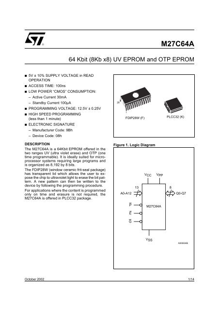
M27C64A64 Kbit (8Kb x8) UV EPROM and OTP EPROM■ 5V ± 10% SUPPLY VOLTAGE in READOPERATION■ ACCESS TIME: 100ns■ LOW POWER “CMOS” CONSUMPTION:– Active Current 30mA– Standby Current 100µA■ PROGRAMMING VOLTAGE: 12.5V ± 0.25V■ HIGH SPEED PROGRAMMING(less than 1 minute)■ ELECTRONIC SIGNATURE– Manufacturer Code: 9Bh– Device Code: 08h281FDIP28W (F)PLCC32 (K)DESCRIPTIONThe M27C64A is a 64Kbit EPROM offered in thetwo ranges UV (ultra violet erase) and OTP (onetime programmable). It is ideally suited for microprocessorsystems requiring large programs andis organized as 8,192 by 8 bits.The FDIP28W (window ceramic frit-seal package)has transparent lid which allows the user to exposethe chip to ultraviolet light to erase the bit pattern.A new pattern can then be written to thedevice by following the programming procedure.For applications where the content is programmedonly on time and erasure is not required, theM27C64A is offered in PLCC32 package.Figure 1. Logic DiagramV CC V PP138A0-A12P M27C64AEGV SSQ0-Q7AI00834BOctober 20021/14
M27C64AFigure 2A. DIP ConnectionsFigure 2B. Pin ConnectionsV PPA12A7A6A5A4A3A2A1A0Q0Q1Q2V SS1234567M27C64A8910111213142827262524232221201918171615AI00835V CCPNCA8A9A11GA10EQ7Q6Q5Q4Q3A6A5A4A3A2A1A0NCQ09A7A12V PPDUV CCPNCQ1Q211732M27C64AV SSDUQ3Q4Q525A8A9A11NCGA10EQ7Q6AI00836Table 1. Signal NamesA0-A12Address InputsQ0-Q7Data OutputsEChip EnableGOutput EnablePProgramV PPProgram SupplyV CCSupply VoltageV SSGroundNCNot Connected InternallyDUDon’t UseDEVICE OPERATIONThe modes of operation of the M27C64A are listedin the Operating Modes table. A single power supplyis required in the read mode. All inputs are TTLlevels except for V PP and 12V on A9 for ElectronicSignature.Read ModeThe M27C64A has two control functions, both ofwhich must be logically active in order to obtaindata at the outputs. Chip Enable (E) is the powercontrol and should be used for device selection.Output Enable (G) is the output control and shouldbe used to gate data to the output pins, independentof device selection. Assuming that the addressesare stable, the address access time(t AVQV ) is equal to the delay from E to output(t ELQV ). Data is available at the output after a delayof t GLQV from the falling edge of G, assuming thatE has been low and the addresses have been stablefor at least t AVQV -t GLQV .2/14
Table 2. Absolute Maximum Ratings (1)M27C64ASymbol Parameter Value UnitT A Ambient Operating Temperature (3) –40 to 125 °CT BIAS Temperature Under Bias –50 to 125 °CT STG Storage Temperature –65 to 150 °CV IO(2) Input or Output Voltage (except A9) –2 to 7 VV CC Supply Voltage –2 to 7 VV A9(2) A9 Voltage –2 to 13.5 VV PP Program Supply Voltage –2 to 14 VNote: 1. Except for the rating "Operating Temperature Range", stresses above those listed in the Table "Absolute Maximum Ratings" maycause permanent damage to the device. These are stress ratings only and operation of the device at these or any other conditionsabove those indicated in the Operating sections of this specification is not implied. Exposure to Absolute Maximum Rating conditionsfor extended periods may affect device reliability. Refer also to the STMicroelectronics SURE Program and other relevant qualitydocuments.2. Minimum DC voltage on Input or Output is –0.5V with possible undershoot to –2.0V for a period less than 20ns. Maximum DCvoltage on Output is V CC +0.5V with possible overshoot to V CC +2V for a period less than 20ns.3. Depends on range.Table 3. Operating ModesMode E G P A9 V PP Q70-Q0Read V IL V IL V IH X V CC Data OutOutput Disable V IL V IH V IH X V CC Hi-ZProgram V IL X V IL Pulse X V PP Data InputVerify V IL V IL V IH X V PP Data OutputProgram Inhibit V IH X X X V PP Hi-ZStandby V IH X X X V CC Hi-ZElectronic Signature V IL V IL V IH V ID V CC CodesNote: X = V IH or V IL , V ID = 12V ± 0.5V.Table 4. Electronic SignatureIdentifier A0 Q7 Q6 Q5 Q4 Q3 Q2 Q1 Q0 Hex DataManufacturer’s Code V IL 1 0 0 1 1 0 1 1 9BhDevice Code V IH 0 0 0 0 1 0 0 0 08h3/14
M27C64ATable 5. AC Measurement ConditionsInput Rise and Fall Times≤ 20nsInput Pulse Voltages 0.4V to 2.4VInput and Output Timing Ref. Voltages 0.8 to 2.0VNote that Output Hi-Z is defined as the point where datais no longer driven.Figure 3. AC Testing Input Output WaveformFigure 4. AC Testing Load Circuit1.3V1N9143.3kΩ2.4V2.0VDEVICEUNDERTESTC L = 100pFOUT0.4V0.8VAI00826C L includes JIG capacitanceAI00828Table 6. Capacitance (1) (T A = 25 °C, f = 1 MHz)Symbol Parameter Test Condition Min Max UnitC IN Input Capacitance V IN = 0V 6 pFC OUT Output Capacitance V OUT = 0V 12 pFNote: 1. Sampled only, not 100% tested.Standby ModeThe M27C64A has a standby mode which reducesthe active current from 30mA to 100µA. TheM27C64A is placed in the standby mode by applyinga CMOS high signal to the E input. When in thestandby mode, the outputs are in a high impedancestate, independent of the G input.Two Line Output ControlBecause EPROMs are usually used in largermemory arrays, this product features a 2 line controlfunction which accommodates the use of multiplememory connection. The two line controlfunction allows:a. the lowest possible memory power dissipation,b. complete assurance that output bus contentionwill not occur.For the most efficient use of these two controllines, E should be decoded and used as the primarydevice selecting function, while G should bemade a common connection to all devices in thearray and connected to the READ line from thesystem control bus. This ensures that all deselectedmemory devices are in their low power standbymode and that the output pins are only activewhen data is required from a particular memorydevice.4/14
Table 7. Read Mode DC Characteristics (1)(T A = 0 to 70 °C or –40 to 85 °C: V CC = 5V ± 10%; V PP = V CC )M27C64ASymbol Parameter Test Condition Min Max UnitI LI Input Leakage Current 0V ≤ V IN ≤ V CC ±10 µAI LO Output Leakage Current 0V ≤ V OUT ≤ V CC ±10 µAI CCSupply CurrentE = V IL , G = V IL ,I OUT = 0mA, f = 5MHz30 mAI CC1 Supply Current (Standby) TTL E = V IH 1 mAI CC2 Supply Current (Standby) CMOS E > V CC – 0.2V 100 µAI PP Program Current V PP = V CC 100 µAV IL Input Low Voltage –0.3 0.8 VV IH(2) Input High Voltage 2 V CC + 1 VV OL Output Low Voltage I OL = 2.1mA 0.4 VV OHOutput High Voltage TTL I OH = –400µA 2.4 VOutput High Voltage CMOS I OH = –100µA V CC – 0.7VNote: 1. V CC must be applied simultaneously with or before V PP and removed simultaneously or after V PP .2. Maximum DC voltage on Output is V CC +0.5V.System ConsiderationsThe power switching characteristics of AdvancedCMOS EPROMs require careful decoupling of thedevices. The supply current, I CC , has three segmentsthat are of interest to the system designer:the standby current level, the active current level,and transient current peaks that are produced bythe falling and rising edges of E. The magnitude ofthe transient current peaks is dependent on thecapacitive and inductive loading of the device atthe output. The associated transient voltage peakscan be suppressed by complying with the two lineoutput control and by properly selected decouplingcapacitors. It is recommended that a 0.1µF ceramiccapacitor be used on every device between V CCand V SS . This should be a high frequency capacitorof low inherent inductance and should beplaced as close to the device as possible. In addition,a 4.7µF bulk electrolytic capacitor should beused between V CC and V SS for every eight devices.The bulk capacitor should be located near thepower supply connection point. The purpose of thebulk capacitor is to overcome the voltage dropcaused by the inductive effects of PCB traces.5/14
M27C64ATable 8. Read Mode AC Characteristics (1)(T A = 0 to 70 °C or –40 to 85 °C: V CC = 5V ± 10%; V PP = V CC )Symbol Alt Parameter Test ConditionM27C64A-10 -15 -20Min Max Min Max Min MaxUnitt AVQV t ACCAddress Valid to OutputValidt ELQV t CEChip Enable Low toOutput Validt GLQV t OEOutput Enable Low toOutput Validt EHQZ(2) t DFChip Enable High toOutput Hi-Zt GHQZ(2) t DFOutput Enable High toOutput Hi-Zt AXQX t OHAddress Transition toOutput TransitionE = V IL , G = V IL 100 150 200 nsG = V IL 100 150 200 nsE = V IL 50 75 80 nsG = V IL 0 50 0 50 0 50 nsE = V IL 0 50 0 50 0 50 nsE = V IL , G = V IL 0 0 0 nsNote: 1. V CC must be applied simultaneously with or before V PP and removed simultaneously or after V PP.2. Sampled only, not 100% tested.Table 9. Read Mode AC Characteristics (1)(T A = 0 to 70 °C or –40 to 85 °C: V CC = 5V ± 10%; V PP = V CC )Symbol Alt Parameter Test ConditionM27C64A-25 -30Min Max Min MaxUnitt AVQV t ACCAddress Valid to OutputValidt ELQV t CEChip Enable Low to OutputValidt GLQV t OEOutput Enable Low toOutput Validt EHQZ(2) t DFChip Enable High toOutput Hi-Zt GHQZ(2) t DFOutput Enable High toOutput Hi-Zt AXQX t OHAddress Transition toOutput TransitionE = V IL , G = V IL 250 300 nsG = V IL 250 300 nsE = V IL 100 120 nsG = V IL 0 60 0 105 nsE = V IL 0 60 0 105 nsE = V IL , G = V IL 0 0 nsNote: 1. V CC must be applied simultaneously with or before V PP and removed simultaneously or after V PP.2. Sampled only, not 100% tested.6/14
M27C64AFigure 5. Read Mode AC WaveformsA0-A12VALIDVALIDtAVQVtAXQXEtGLQVtEHQZGQ0-Q7tELQVtGHQZHi-ZAI00778B7/14
M27C64ATable 10. Programming Mode DC Characteristics (1)(T A = 25 °C; V CC = 6V ± 0.25V; V PP = 12.5V ± 0.25V)Symbol Parameter Test Condition Min Max UnitI LI Input Leakage Current V IL ≤ V IN ≤ V IH ±10 µAI CC Supply Current 30 mAI PP Program Current E = V IL 30 mAV IL Input Low Voltage –0.3 0.8 VV IH Input High Voltage 2 V CC + 0.5 VV OL Output Low Voltage I OL = 2.1mA 0.4 VV OH Output High Voltage TTL I OH = –400µA 2.4 VV ID A9 Voltage 11.5 12.5 VNote: 1. V CC must be applied simultaneously with or before V PP and removed simultaneously or after V PP.Table 11. Programming Mode AC Characteristics (1)(T A = 25 °C; V CC = 6V ± 0.25V; V PP = 12.5V ± 0.25V)Symbol Alt Parameter Test Condition Min Max Unitt AVPL t AS Address Valid to Program Low 2 µst QVPL t DS Input Valid to Program Low 2 µst VPHPL t VPS V PP High to Program Low 2 µst VCHPL t VCS V CC High to Program Low 2 µst ELPL t CES Chip Enable Low to Program Low 2 µst PLPH t PWProgram Pulse Width (Initial) 0.95 1.05 msProgram Pulse Width (Over Program) 2.85 78.75 mst PHQX t DH Program High to Input Transition 2 µst QXGL t OES Input Transition to Output Enable Low 2 µst GLQV t OE Output Enable Low to Output Valid 100 nst GHQZ(2) t DFP Output Enable High to Output Hi-Z 0 130 nst GHAX t AHOutput Enable High to AddressTransition0 nsNote: 1. V CC must be applied simultaneously with or before V PP and removed simultaneously or after V PP.2. Sampled only, not 100% tested.ProgrammingWhen delivered (and after each erasure for UVEPROM), all bits of the M27C64A are in the "1"state. Data is introduced by selectively programming"0"s into the desired bit locations. Althoughonly "0"s will be programmed, both "1"s and "0"scan be present in the data word. The only way tochange a "0" to a "1" is by die exposition to ultravioletlight (UV EPROM). The M27C64A is in theprogramming mode when V PP input is at 12.5V, Eis at V IL and P is pulsed to V IL . The data to be programmedis applied to 8 bits in parallel to the dataoutput pins. The levels required for the addressand data inputs are TTL. V CC is specified to be 6V± 0.25V.8/14
M27C64AFigure 6. Programming and Verify Modes AC WaveformsA0-A12VALIDtAVPLQ0-Q7DATA INDATA OUTtQVPLtPHQXV PPtVPHPLtGLQVtGHQZV CCtVCHPLtGHAXEPtELPLtPLPHtQXGLGPROGRAMVERIFYAI00779Figure 7. Programming FlowchartNOYES++n> 25FAILV CC = 6V, V PP = 12.5VNOn = 1P = 1ms PulseVERIFYLastAddrYESP = 3ms Pulse by nYESNOCHECK ALL BYTES1st: V CC = 6V2nd: V CC = 4.2V++ AddrHigh Speed ProgrammingThe high speed programming algorithm, describedin the flowchart, rapidly programs theM27C64A using an efficient and reliable method,particularly suited to the production programmingenvironment. An individual device will take around1 minute to program.Program InhibitProgramming of multiple M27C64A in parallel withdifferent data is also easily accomplished. Exceptfor E, all like inputs including G of the parallelM27C64A may be common. A TTL low level pulseapplied to a M27C64A P input, with E low and V PPat 12.5V, will program that M27C64A. A high levelE input inhibits the other M27C64A from being programmed.Program VerifyA verify (read) should be performed on the programmedbits to determine that they were correctlyprogrammed. The verify is accomplished with Eand G at V IL , P at V IH , V PP at 12.5V and V CC at 6V.AI011679/14
M27C64AElectronic SignatureThe Electronic Signature (ES) mode allows thereading out of a binary code from an EPROM thatwill identify its manufacturer and type. This modeis intended for use by programming equipment toautomatically match the device to be programmedwith its corresponding programming algorithm.The ES mode is functional in the 25°C ± 5°C ambienttemperature range that is required when programmingthe M27C64A. To activate the ESmode, the programming equipment must force11.5V to 12.5V on address line A9 of theM27C64A, with V PP = V CC = 5V. Two identifierbytes may then be sequenced from the device outputsby toggling address line A0 from V IL to V IH . Allother address lines must be held at V IL duringElectronic Signature mode.Byte 0 (A0 = V IL ) represents the manufacturercode and byte 1 (A0=V IH ) the device identifiercode. For the STMicroelectronics M27C64A,these two identifier bytes are given in Table 4 andcan be read-out on outputs Q7 to Q0.ERASURE OPERATION (applies to UV EPROM)The erasure characteristics of the M27C64A issuch that erasure begins when the cells are exposedto light with wavelengths shorter than approximately4000 Å. It should be noted thatsunlight and some type of fluorescent lamps havewavelengths in the 3000-4000 Å range. Researchshows that constant exposure to room level fluorescentlighting could erase a typical M27C64A inabout 3 years, while it would take approximately 1week to cause erasure when exposed to directsunlight. If the M27C64A is to be exposed to thesetypes of lighting conditions for extended periods oftime, it is suggested that opaque labels be put overthe M27C64A window to prevent unintentionalerasure. The recommended erasure procedure forthe M27C64A is exposure to short wave ultravioletlight which has a wavelength of 2537 Å. The integrateddose (i.e. UV intensity x exposure time) forerasure should be a minimum of 15 W-sec/cm 2 .The erasure time with this dosage is approximately15 to 20 minutes using an ultraviolet lamp with12000 µW/cm 2 power rating. The M27C64Ashould be placed within 2.5 cm (1 inch) of the lamptubes during the erasure. Some lamps have a filteron their tubes which should be removed beforeerasure.10/14
M27C64ATable 12. Ordering Information SchemeExample: M27C64A -10 K 1 TRDevice TypeM27Supply VoltageC = 5V ±10%Device Function64A = 64 Kbit (8Kb x8)Speed-10 = 100 ns-15 = 150 ns-20 = 200 ns-25 = 250 ns-30 = 300 nsPackageF = FDIP28WK = PLCC32Temperature Range1 = 0 to 70 °C6 = –40 to 85 °COptionsX = Additional Burn-inTR = Tape & Reel PackingFor a list of available options (Speed, Package, etc...) or for further information on any aspect of this device,please contact the STMicroelectronics Sales Office nearest to you.Table 13. Revision HistoryDate Version Revision DetailsMarch 1998 1.0 First Issue25-Sep-2000 2.0 AN620 Reference removed29-Oct-2002 2.1100ns speed class addedFDIP28W mechanical data clarified (Table 14)PLCC32 mechanical data and drawing clarified (Table 15, Figure 9)11/14
M27C64ATable 14. FDIP28W - 28 pin Ceramic Frit-seal DIP, with window, Package Mechanical DataSymbolmillimetersinchesTyp Min Max Typ Min MaxA 5.72 0.225A1 0.51 1.40 0.020 0.055A2 3.91 4.57 0.154 0.180A3 3.89 4.50 0.153 0.177B 0.41 0.56 0.016 0.022B1 1.45 – – 0.057 – –C 0.23 0.30 0.009 0.012D 36.50 37.34 1.437 1.470D2 33.02 – – 1.300 – –E 15.24 – – 0.600 – –E1 13.06 13.36 0.514 0.526e 2.54 – – 0.100 – –eA 14.99 – – 0.590 – –eB 16.18 18.03 0.637 0.710L 3.18 4.10 0.125 0.161S 1.52 2.49 0.060 0.098∅ 7.11 – – 0.280 – –α 4° 11° 4° 11°N 28 28Figure 8. FDIP28W - 28 pin Ceramic Frit-seal DIP, with window, Package OutlineA2A3AA1B1 B eD2LαeAeBCSDN∅E1E1FDIPW-aDrawing is not to scale.12/14
M27C64ATable 15. PLCC32 - 32 lead Plastic Leaded Chip Carrier, Package Mechanical DataSymbolmillimetersinchesTyp Min Max Typ Min MaxA 3.18 3.56 0.125 0.140A1 1.53 2.41 0.060 0.095A2 0.38 – 0.015 –B 0.33 0.53 0.013 0.021B1 0.66 0.81 0.026 0.032CP 0.10 0.004D 12.32 12.57 0.485 0.495D1 11.35 11.51 0.447 0.453D2 4.78 5.66 0.188 0.223D3 7.62 – – 0.300 – –E 14.86 15.11 0.585 0.595E1 13.89 14.05 0.547 0.553E2 6.05 6.93 0.238 0.273E3 10.16 – – 0.400 – –e 1.27 – – 0.050 – –F 0.00 0.13 0.000 0.005N 32 32R 0.89 0.035Figure 9. PLCC32 - 32 lead Plastic Leaded Chip Carrier, Package OutlineDD1A1A21 NE2B1E3E1 EF0.51 (.020)E2Be1.14 (.045)D3ARCPD2Drawing is not to scale.D2PLCC-A13/14
M27C64AInformation furnished is believed to be accurate and reliable. However, STMicroelectronics assumes no responsibility for the consequencesof use of such information nor for any infringement of patents or other rights of third parties which may result from its use. No license is grantedby implication or otherwise under any patent or patent rights of STMicroelectronics. Specifications mentioned in this publication are subjectto change without notice. This publication supersedes and replaces all information previously supplied. STMicroelectronics products are notauthorized for use as critical components in life support devices or systems without express written approval of STMicroelectronics.The ST logo is registered trademark of STMicroelectronicsAll other names are the property of their respective owners© 2002 STMicroelectronics - All Rights ReservedSTMicroelectronics GROUP OF COMPANIESAustralia - Brazil - Canada - China - Finland - France - Germany - Hong Kong - India - Israel - Italy - Japan - Malaysia - Malta -Morocco - Singapore - Spain - Sweden - Switzerland - United Kingdom - United Stateswww.st.com14/14