74ACT74 - Futurlec
74ACT74 - Futurlec
74ACT74 - Futurlec

You also want an ePaper? Increase the reach of your titles
YUMPU automatically turns print PDFs into web optimized ePapers that Google loves.
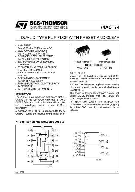
<strong>74ACT74</strong>DUAL D-TYPE FLIP FLOP WITH PRESET AND CLEAR■■■■■■■■■HIGH SPEED:fMAX = 250 MHz (TYP.) at VCC =5VLOW POWER DISSIPATION:ICC =4µA (MAX.) at TA =25 o CCOMPATIBLE WITH TTL OUTPUTSV IH =2V(MIN),V IL = 0.8V (MAX)50Ω TRANSMISSION LINE DRIVINGCAPABILITYSYMMETRICAL OUTPUT IMPEDANCE:|I OH |=I OL =24mA(MIN)BALANCED PROPAGATION DELAYS:tPLH ≅ tPHLOPERATING VOLTAGE RANGE:VCC (OPR) = 4.5V to 5.5VPIN AND FUNCTION COMPATIBLE WITH74 SERIES 74IMPROVED LATCH-UP IMMUNITYDESCRIPTIONThe ACT74 is an advanced high-speed CMOSOCTAL D-TYPE FLIP FLOP WITH PRESET ANDCLEAR fabricated with sub-micron silicon gateand double-layer metal wiring C 2 MOStechnology.A signal on the D INPUT is transferred to the QOUTPUT during the positive going transition ofB(Plastic Package)M(Micro Package)ORDER CODES :<strong>74ACT74</strong>B<strong>74ACT74</strong>Mthe clock pulse.CLEAR and PRESET are independent of theclock and accomplished by a low setting on theappropriate input.It is ideal for low power applications mantaininghigh speed operation similar to equivalent BipolarSchottky TTL.The device is designed to interface directly HighSpeed CMOS systems with TTL, NMOS andCMOS output voltage levels.All inputs and outputs are equipped withprotection circuits against static discharge, givingthem 2KV ESD immunity and transient excessvoltage.PIN CONNECTION AND IEC LOGIC SYMBOLSApril 19971/11
<strong>74ACT74</strong>INPUT AND OUTPUT EQUIVALENT CIRCUITPIN DESCRIPTIONPIN No SYMBOL NAME AND FUNCTION1, 13 1CLR,2CLRAsyncronous Reset -Direct Input2, 12 1D, 2D Data Inputs3, 11 1CK, 2CK Clock Input(LOW-to-HIGH, Edge-Triggered)4, 10 1PR, 2PR Asyncronous Set - DirectInput5, 9 1Q, 2Q True Flip-Flop Outputs6, 8 1Q, 2Q Complement Flip-FlopOutputs7 GND Ground (0V)14 VCC Positive Supply VoltageTRUTH TABLEINPUTS OUTPUTS FUNCTIONCLR PR D CK Q QL H X X L H CLEARH L X X H L PRESETL L X X H HH H L L HH H H H LH H X Q n Q n NO CHANGEX:Don’t CareLOGIC DIAGRAMSThis logic diagram has not be used to estimate propagation delays2/11
<strong>74ACT74</strong>ABSOLUTE MAXIMUM RATINGSSymbol Parameter Value UnitV CC Supply Voltage -0.5 to +7 VVI DC Input Voltage -0.5 to VCC + 0.5 VVO DC Output Voltage -0.5 to VCC + 0.5 VI IK DC Input Diode Current ± 20 mAI OK DC Output Diode Current ± 20 mAIO DC Output Current ± 50 mAI CC or I GND DC V CC or Ground Current ± 200 mATstg Storage Temperature -65 to +150TL Lead Temperature (10 sec) 300o CAbsolute Maximum Ratings are those values beyond which damage to the device may occur. Functional operation under these condition is not implied.o CRECOMMENDED OPERATING CONDITIONSSymbol Parameter Value UnitVCC Supply Voltage 4.5 to 5.5 VVI Input Voltage 0 to VCC VVO Output Voltage 0 to VCC VT op Operating Temperature: -40 to +85o Cdt/dv Input Rise and Fall Time V CC = 4.5 to 5.5V (note 1) 8 ns/V1) V IN from 0.8 V to 2.0 V3/11
<strong>74ACT74</strong>DC SPECIFICATIONSSymbol Parameter Test Conditions Value UnitV CCT A =25 o C -40 to 85 o C(V)Min. Typ. Max. Min. Max.VIH High Level Input Voltage 4.5 VO = 0.1 V or 2.0 1.5 2.05.5 V CC - 0.1 V 2.0 1.5 2.0VV IL Low Level Input Voltage 4.5 V O = 0.1 V or1.5 0.8 0.85.5VCC - 0.1 V1.5 0.8 0.8VV OH High Level Output4.5VI (*) I O =-50 µA 4.4 4.49 4.4=Voltage5.5 V IH or I O =-50 µA 5.4 5.49 5.4V4.5 V IL IO=-24 mA 3.86 3.765.5 I O =-24 mA 4.86 4.76VOL Low Level Output4.5V (*) IO=50 µA 0.001 0.1 0.1VoltageI =5.5 V IH or IO=50 mA 0.001 0.1 0.1V4.5 VIL IO=24 mA 0.36 0.445.5 I O =24 mA 0.36 0.44I I Input Leakage Current 5.5 V I =V CC or GND ±0.1 ±1 µAICCT Max ICC /Input 5.5 VI =VCC -2.1 V 0.6 1.5 mAI CC Quiescent Supply5.5 V I =V CC or GND 4 40 µACurrentIOLD Dynamic Output Current 5.5 VOLD = 1.65 V max 75 mAI OHD(note 1, 2)V OHD = 3.85 V min -75 mA1) Maximum test duration 2ms, one output loaded at time2) Incident wave switching is guaranteed on transmission lines with impedances as low as 50 Ω.(*) All outputs loaded.4/11
<strong>74ACT74</strong>AC ELECTRICAL CHARACTERISTICS (CL = 50 pF, RL = 500 Ω, Input tr =tf =3 ns)Symbol Parameter Test Condition Value UnitV CCT A =25 o C -40 to 85 o C(V)Min. Typ. Max. Min. Max.tPLHtPHLPropagation Delay TimeCK to Q5.0 (*) 5.0 10.0 11.0 nstPLHt PHLt wt st htremfMAXPropagation Delay TimePR or CLR to Q or QCK Pulse Width, HIGHor LOWSetup Time Q to CKHIGH or LOWHold Time Q to CKHIGH or LOWRemoval Time PR orCLR to CKMaximim ClockFrequency(*) Voltage range is 5V ± 0.5V5.0 (*) 5.0 10.0 11.0 ns5.0 (*) 1.5 5.0 6.0 ns5.0 (*) 0.5 3.0 3.5 ns5.0 (*) -0.5 1.0 1.0 ns5.0 (*) -0.7 1.0 1.0 ns5.0 (*) 100 250 85 MHzCAPACITIVE CHARACTERISTICSSymbol Parameter Test Conditions Value UnitV CCT A =25 o C -40 to 85 o C(V)Min. Typ. Max. Min. Max.C IN Input Capacitance 5.0 4 pFC PD Power Dissipation5.0 43 pFCapacitance (note 1)1) CPD is defined as the value of the IC’s internal equivalent capacitance which is calculated from the operating current consumption without load. (Refer toTest Circuit). Average operating current can be obtained by the following equation. I CC(opr) = C PD • V CC •f IN +I CC/n (per circuit)5/11
<strong>74ACT74</strong>TEST CIRCUITCL = 50 pF or equivalent (includes jig and probe capacitance)R L =R 1 = 500Ω or equivalentRT =ZOUT of pulse generator (typically 50Ω)WAVEFORM 1: PROPAGATION DELAYS, SETUP AND HOLD TIMES (f=1MHz; 50% duty cycle)6/11
<strong>74ACT74</strong>WAVEFORM 2: PROPAGATION DELAYS (f=1MHz; 50% duty cycle)7/11
<strong>74ACT74</strong>WAVEFORM 3: RECOVERY TIMES (f=1MHz; 50% duty cycle)WAVEFORM 3: PULSE WIDTH8/11
<strong>74ACT74</strong>Plastic DIP14 MECHANICAL DATADIM.mminchMIN. TYP. MAX. MIN. TYP. MAX.a1 0.51 0.020B 1.39 1.65 0.055 0.065b 0.5 0.020b1 0.25 0.010D 20 0.787E 8.5 0.335e 2.54 0.100e3 15.24 0.600F 7.1 0.280I 5.1 0.201L 3.3 0.130Z 1.27 2.54 0.050 0.100P001A9/11
<strong>74ACT74</strong>SO14 MECHANICAL DATADIM.mminchMIN. TYP. MAX. MIN. TYP. MAX.A 1.75 0.068a1 0.1 0.2 0.003 0.007a2 1.65 0.064b 0.35 0.46 0.013 0.018b1 0.19 0.25 0.007 0.010C 0.5 0.019c145 (typ.)D 8.55 8.75 0.336 0.344E 5.8 6.2 0.228 0.244e 1.27 0.050e3 7.62 0.300F 3.8 4.0 0.149 0.157G 4.6 5.3 0.181 0.208L 0.5 1.27 0.019 0.050M 0.68 0.026S8 (max.)P013G10/11
<strong>74ACT74</strong>Information furnished is believed to be accurate and reliable. However, SGS-THOMSON Microelectronics assumes no responsability for theconsequences of use of such information nor for any infringement of patents or other rights of third parties which may results from its use. Nolicense is granted by implication or otherwise under any patent or patent rights of SGS-THOMSON Microelectronics. Specifications mentionedin this publication are subject to change without notice. This publication supersedes and replaces all information previously supplied.SGS-THOMSON Microelectronics products are not authorized for use as critical components in life supportdevices or systems without expresswritten approval of SGS-THOMSON Microelectonics.© 1997 SGS-THOMSON Microelectronics - Printed in Italy - All Rights ReservedSGS-THOMSON Microelectronics GROUP OF COMPANIESAustralia - Brazil - Canada - China - France - Germany - Hong Kong - Italy - Japan- Korea - Malaysia - Malta - Morocco - The Netherlands -Singapore - Spain - Sweden - Switzerland - Taiwan - Thailand - United Kingdom - U.S.A.11/11