P89C51RB2/P89C51RC2/P89C51RD2 80C51 8-bit Flash ...
P89C51RB2/P89C51RC2/P89C51RD2 80C51 8-bit Flash ...
P89C51RB2/P89C51RC2/P89C51RD2 80C51 8-bit Flash ...

Create successful ePaper yourself
Turn your PDF publications into a flip-book with our unique Google optimized e-Paper software.
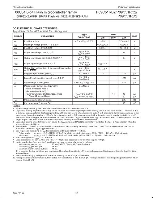
Philips Semiconductors<strong>80C51</strong> 8-<strong>bit</strong> <strong>Flash</strong> microcontroller family16KB/32KB/64KB ISP/IAP <strong>Flash</strong> with 512B/512B/1KB RAMPreliminary specification<strong>P89C51RB2</strong>/<strong>P89C51RC2</strong>/<strong>P89C51RD2</strong>DC ELECTRICAL CHARACTERISTICST amb = 0°C to +70°C or –40°C to +85°C; 5 V ±10%; V SS = 0 VSYMBOLPARAMETERTESTLIMITSCONDITIONS MIN TYP 1 MAXUNITV IL Input low voltage 4.5 V < V CC < 5.5 V –0.5 0.2V CC –0.1 VV IH Input high voltage (ports 0, 1, 2, 3, EA) 0.2V CC +0.9 V CC +0.5 VV IH1 Input high voltage, XTAL1, RST 0.7V CC V CC +0.5 VV OL Output low voltage, ports 1, 2, 3 8 V CC = 4.5 VI OL = 1.6 mA 2 0.4 VV OL1 Output low voltage, port 0, ALE, PSEN 7, 8 V CC = 4.5 VI OL = 3.2 mA 2 0.4 VV OH Output high voltage, ports 1, 2, 3 3 V CC = 4.5 VI OH = –30 µAV OH1Output high voltage (port 0 in external bus mode),ALE 9 , PSEN 3V CC = 4.5 VI OH = –3.2 mAV CC – 0.7V CC – 0.7I IL Logical 0 input current, ports 1, 2, 3 V IN = 0.4 V –1 –75 µAI TL Logical 1-to-0 transition current, ports 1, 2, 3 6 V IN = 2.0 VSee Note 4–650 µAI LI Input leakage current, port 0 0.45 < V IN < V CC – 0.3 ±10 µAI CC Power supply current (see Figure 36): See Note 5Active mode (see Note 5)Idle mode (see Note 5)Power-down mode or clock stopped (seeT amb = 0°C to 70°C 100 pF), the noise pulse on the ALE pin may exceed 0.8 V. In such cases, it may be desirable to qualifyALE with a Schmitt Trigger, or use an address latch with a Schmitt Trigger STROBE input. I OL can exceed these conditions provided that nosingle output sinks more than 5 mA and no more than two outputs exceed the test conditions.3. Capacitive loading on ports 0 and 2 may cause the V OH on ALE and PSEN to momentarily fall below the V CC –0.7 specification when theaddress <strong>bit</strong>s are stabilizing.4. Pins of ports 1, 2 and 3 source a transition current when they are being externally driven from 1 to 0. The transition current reaches itsmaximum value when V IN is approximately 2 V.5. See Figures 39 through 42 for I CC test conditions and Figure 36 for I CC vs Freq.Active mode: I CC(MAX) = (1.8 × FREQ. + 20)mA for all devices, in 6 clock mode; (0.9 × FREQ. + 20)mA in 12 clock mode.Idle mode: I CC(MAX) = (0.7 × FREQ. +1.0)mA in 6 clock mode; (0.35 × FREQ. +1.0)mA in 12 clock mode.6. This value applies to T amb = 0°C to +70°C.7. Load capacitance for port 0, ALE, and PSEN = 100 pF, load capacitance for all other outputs = 80 pF.8. Under steady state (non-transient) conditions, I OL must be externally limited as follows:Maximum I OL per port pin: 15 mA (*NOTE: This is 85°C specification.)Maximum I OL per 8-<strong>bit</strong> port: 26 mAMaximum total I OL for all outputs: 71 mAIf I OL exceeds the test condition, V OL may exceed the related specification. Pins are not guaranteed to sink current greater than the listedtest conditions.9. ALE is tested to V OH1 , except when ALE is off then V OH is the voltage specification.10. Pin capacitance is characterized but not tested. Pin capacitance is less than 25 pF. Pin capacitance of ceramic package is less than 15 pF(except EA is 25 pF).VV1999 Nov 22 32