P89C51RB2/P89C51RC2/P89C51RD2 80C51 8-bit Flash ...
P89C51RB2/P89C51RC2/P89C51RD2 80C51 8-bit Flash ...
P89C51RB2/P89C51RC2/P89C51RD2 80C51 8-bit Flash ...

Create successful ePaper yourself
Turn your PDF publications into a flip-book with our unique Google optimized e-Paper software.
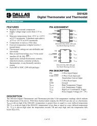
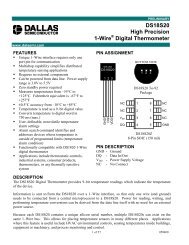
Philips Semiconductors<strong>80C51</strong> 8-<strong>bit</strong> <strong>Flash</strong> microcontroller family16KB/32KB/64KB ISP/IAP <strong>Flash</strong> with 512B/512B/1KB RAMPreliminary specification<strong>P89C51RB2</strong>/<strong>P89C51RC2</strong>/<strong>P89C51RD2</strong>PIN DESCRIPTIONSMNEMONICPIN NUMBERPDIP PLCC PQFPTYPENAME AND FUNCTIONV SS 20 22 16 I Ground: 0 V reference.V CC 40 44 38 I Power Supply: This is the power supply voltage for normal, idle, and power-downoperation.P0.0–0.7 39–32 43–36 37–30 I/O Port 0: Port 0 is an open-drain, bidirectional I/O port. Port 0 pins that have 1swritten to them float and can be used as high-impedance inputs. Port 0 is also themultiplexed low-order address and data bus during accesses to external programand data memory. In this application, it uses strong internal pull-ups when emitting 1s.P1.0–P1.7 1–8 2–9 40–44,1–3I/OPort 1: Port 1 is an 8-<strong>bit</strong> bidirectional I/O port with internal pull-ups on all pinsexcept P1.6 and P1.7 which are open drain. Port 1 pins that have 1s written to themare pulled high by the internal pull-ups and can be used as inputs. As inputs, port 1pins that are externally pulled low will source current because of the internalpull-ups. (See DC Electrical Characteristics: I IL ).Alternate functions for 89C51RB2/RC2/RD2 Port 1 include:1 2 40 I/O T2 (P1.0): Timer/Counter 2 external count input/Clockout (see ProgrammableClock-Out)2 3 41 I T2EX (P1.1): Timer/Counter 2 Reload/Capture/Direction Control3 4 42 I ECI (P1.2): External Clock Input to the PCA4 5 43 I/O CEX0 (P1.3): Capture/Compare External I/O for PCA module 05 6 44 I/O CEX1 (P1.4): Capture/Compare External I/O for PCA module 16 7 1 I/O CEX2 (P1.5): Capture/Compare External I/O for PCA module 27 8 2 I/O CEX3 (P1.6): Capture/Compare External I/O for PCA module 38 9 3 I/O CEX4 (P1.7): Capture/Compare External I/O for PCA module 4P2.0–P2.7 21–28 24–31 18–25 I/O Port 2: Port 2 is an 8-<strong>bit</strong> bidirectional I/O port with internal pull-ups. Port 2 pins thathave 1s written to them are pulled high by the internal pull-ups and can be used asinputs. As inputs, port 2 pins that are externally being pulled low will source currentbecause of the internal pull-ups. (See DC Electrical Characteristics: I IL ). Port 2emits the high-order address byte during fetches from external program memoryand during accesses to external data memory that use 16-<strong>bit</strong> addresses (MOVX@DPTR). In this application, it uses strong internal pull-ups when emitting 1s.During accesses to external data memory that use 8-<strong>bit</strong> addresses (MOV @Ri),port 2 emits the contents of the P2 special function register.P3.0–P3.7 10–17 11,13–195, 7–13 I/O Port 3: Port 3 is an 8-<strong>bit</strong> bidirectional I/O port with internal pull-ups. Port 3 pins thathave 1s written to them are pulled high by the internal pull-ups and can be used asinputs. As inputs, port 3 pins that are externally being pulled low will source currentbecause of the pull-ups. (See DC Electrical Characteristics: I IL ). Port 3 also servesthe special features of the 89C51RB2/RC2/RD2, as listed below:10 11 5 I RxD (P3.0): Serial input port11 13 7 O TxD (P3.1): Serial output port12 14 8 I INT0 (P3.2): External interrupt13 15 9 I INT1 (P3.3): External interrupt14 16 10 I T0 (P3.4): Timer 0 external input15 17 11 I T1 (P3.5): Timer 1 external input16 18 12 O WR (P3.6): External data memory write strobe17 19 13 O RD (P3.7): External data memory read strobeRST 9 10 4 I Reset: A high on this pin for two machine cycles while the oscillator is running,resets the device. An internal resistor to V SS permits a power-on reset using onlyan external capacitor to V CC .ALE 30 33 27 O Address Latch Enable: Output pulse for latching the low byte of the addressduring an access to external memory. In normal operation, ALE is emitted twiceevery machine cycle, and can be used for external timing or clocking. Note that oneALE pulse is skipped during each access to external data memory. ALE can bedisabled by setting SFR auxiliary.0. With this <strong>bit</strong> set, ALE will be active only during aMOVX instruction.1999 Nov 22 6