

Biennial Report 2016/2017

Create successful ePaper yourself
Turn your PDF publications into a flip-book with our unique Google optimized e-Paper software.
<strong>Report</strong>s<br />
Reactive Ion Beam Etching for Ultraprecise Fabrication of Optical<br />
Elements: A Progress <strong>Report</strong><br />
R. Fechner, A. Finzel, G. Dornberg, M. Mitzschke, S. Görsch, A. Nickel, F. Frost<br />
in collaboration with<br />
F. Koch, D. Lehr, O. Schönbrodt, T. Glaser, Carl Zeiss Jena GmbH, Microstructured Optics, Germany<br />
Introduction<br />
(Reactive) ion beam etching ((R)IBE) becomes<br />
more and more a versatile and indispensable<br />
technology step in the fabrication chain of high<br />
precision optical elements. An example for the<br />
crucial importance of RIBE is the pattern transfer<br />
of 3D resist or metal masks into hard optical<br />
materials, especially for the fabrication of highend<br />
optical diffraction gratings [1,2].<br />
Today gratings can be manufactured using<br />
various sophisticated techniques, e. g.,<br />
interference lithography, mechanical ruling,<br />
volume holography, laser direct writing<br />
lithography, electron-beam writing, and Talbot<br />
lithography. While for some applications the resist<br />
grating is sufficient, the vast majority of<br />
applications demands grating patterns to be<br />
transferred into glass, silicon, metals, or other<br />
substrate materials. Due to the very high flexibility<br />
and degree of freedom RIBE is predestined for<br />
this. Thus, due to process optimized gas mixture<br />
used for etching, the selectivity (ratio of the etch<br />
rates of the substrate material related to the etch<br />
rate of the mask material) can be varied over<br />
several orders of magnitude making it possible to<br />
compress or stretch surface profiles during the<br />
pattern transfer, according to the respective<br />
optical application. Owing to the spatial separation<br />
of ion generation and substrate, RIBE steps at<br />
non-normal ion incidence additionally offers a<br />
targeted alteration of the surface profile, e. g., the<br />
implementation of undercut patterns or lanted<br />
gratings or the realization of blazed gratings<br />
starting with symmetrical mask profiles. Moreover,<br />
RIBE is a key step in the ion beam planarization<br />
technique, for example, for smoothing of diamond<br />
turned metal surfaces with sub-nm roughness<br />
values [3].<br />
In this report research activities in the core area<br />
Ion Beam assisted Technologies will be<br />
summarized. The work focused mainly on<br />
improvement of technical infrastructure, the<br />
integration and further optimization of in-situ<br />
measurement techniques, the implementation of<br />
sophisticated processing algorithms, which allow<br />
a RIBE processing of workpieces larger than the<br />
extension of the ion beam and the development of<br />
RIBE processing steps for high-end diffraction<br />
gratings.<br />
Technical Infrastructure<br />
The improvement in the technical infrastructure<br />
was one of the key issue in recent years. Thanks<br />
to the funding provided by BMBF within the<br />
SHAPION project [4] and with the additional help<br />
of European Regional Development funding and<br />
funding from the Free State of Saxony a total of<br />
three new RIBE facilities (ISA 200, SHAPION,<br />
RIBE 450) could be taken into operation recently.<br />
All RIBE systems are equipped with Kaufmantype<br />
ion sources (grid apertures of 180 mm),<br />
configured for Fluorine-based etching gases, and<br />
were partially upgraded with different optical and<br />
mass spectroscopic in-situ measurement<br />
technologies which guarantee for a high process<br />
stability and reliability. All machines allow a base<br />
pressure of 1 × 10 -7 mbar and are able to execute<br />
process variable user defined recipes. Both ISA<br />
200 as well as the SHAPION RIBE plant enable<br />
the processing of workpieces up to 245 mm in<br />
diameter. With the former also a defined ion beam<br />
sputter deposition of, e.g. metals, during etching<br />
is possible in order to investigate ion beam driven<br />
self-organized pattern formation processes with<br />
and without co-deposition. Within the extended<br />
research infrastructure a new state-of-the-art<br />
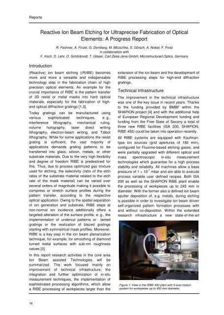
Figure 1: View in the RIBE 450 plant with 5-axis-motion<br />
system for workpieces up to 450 mm diameter.<br />
18