

Biennial Report 2016/2017

Create successful ePaper yourself
Turn your PDF publications into a flip-book with our unique Google optimized e-Paper software.
<strong>Report</strong>s<br />
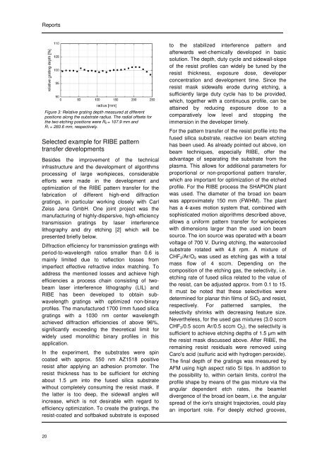
Figure 3: Relative grating depth measured at different<br />
positions along the substrate radius. The radial offsets for<br />
the two etching positions were R 0 = 107.9 mm and<br />
R 1 = 260.6 mm, respectively.<br />
Selected example for RIBE pattern<br />
transfer developments<br />
Besides the improvement of the technical<br />
infrastructure and the development of algorithms<br />
processing of large workpieces, considerable<br />
efforts were made in the development and<br />
optimization of the RIBE pattern transfer for the<br />
fabrication of different high-end diffraction<br />
gratings, in particular working closely with Carl<br />
Zeiss Jena GmbH. One joint project was the<br />
manufacturing of highly-dispersive, high-efficiency<br />
transmission gratings by laser interference<br />
lithography and dry etching [2] which will be<br />
presented briefly below.<br />
Diffraction efficiency for transmission gratings with<br />
period-to-wavelength ratios smaller than 0.6 is<br />
mainly limited due to reflection losses from<br />
imperfect effective refractive index matching. To<br />
address the mentioned losses and achieve high<br />
efficiencies a process chain consisting of twobeam<br />
laser interference lithography (LIL) and<br />
RIBE has been developed to obtain subwavelength<br />
gratings with optimized non-binary<br />
profiles. The manufactured 1700 l/mm fused silica<br />
gratings with a 1030 nm center wavelength<br />
achieved diffraction efficiencies of above 96%,<br />
significantly exceeding the theoretical limit for<br />
widely used monolithic binary profiles in this<br />
application.<br />
In the experiment, the substrates were spin<br />
coated with approx. 550 nm AZ1518 positive<br />
resist after applying an adhesion promoter. The<br />
resist thickness has to be sufficient for etching<br />
about 1.5 µm into the fused silica substrate<br />
without completely consuming the resist mask. If<br />
the latter is too deep, the sidewall angles will<br />
increase, which is not desirable with regard to<br />
efficiency optimization. To create the gratings, the<br />
resist-coated and softbaked substrate is exposed<br />
to the stabilized interference pattern and<br />
afterwards wet-chemically developed in basic<br />
solution. The depth, duty cycle and sidewall-slope<br />
of the resist profiles can widely be tuned by the<br />
resist thickness, exposure dose, developer<br />
concentration and development time. Since the<br />
resist mask sidewalls erode during etching, a<br />
sufficiently large duty cycle has to be provided,<br />
which, together with a continuous profile, can be<br />
attained by reducing exposure dose to a<br />
comparatively low level and stopping the<br />
immersion in the developer timely.<br />
For the pattern transfer of the resist profile into the<br />
fused silica substrate, reactive ion beam etching<br />
has been used. As already pointed out above, ion<br />
beam techniques, especially RIBE, offer the<br />
advantage of separating the substrate from the<br />
plasma. This allows for additional parameters for<br />
proportional or non-proportional pattern transfer,<br />
which are important for optimization of the etched<br />
profile. For the RIBE process the SHAPION plant<br />
was used. The diameter of the broad ion beam<br />
was approximately 150 mm (FWHM). The plant<br />
has a 4-axes motion system that, combined with<br />
sophisticated motion algorithms described above,<br />
allows a uniform pattern transfer for workpieces<br />
with dimensions larger than the used ion beam<br />
source. The ion source was operated with a beam<br />
voltage of 700 V. During etching, the watercooled<br />
substrate rotated with 4.8 rpm. A mixture of<br />
CHF 3 /Ar/O 2 was used as etching gas with a total<br />
mass flow of 4 sccm. Depending on the<br />
composition of the etching gas, the selectivity, i.e.<br />
etching rate of fused silica related to the value of<br />
the resist, can be adjusted approx. from 0.1 to 15.<br />
It must be noted that these selectivities were<br />
determined for planar thin films of SiO 2 and resist,<br />
respectively. For patterned samples, the<br />
selectivity shrinks with decreasing feature size.<br />
Nevertheless, for the used gas mixtures (3.0 sccm<br />
CHF 3 /0.5 sccm Ar/0.5 sccm O 2 ), the selectivity is<br />
sufficient to achieve etching depths of 1.5 µm with<br />
the resist mask discussed above. After RIBE, the<br />
remaining resist residuals were removed using<br />
Caro's acid (sulfuric acid with hydrogen peroxide).<br />
The final depth of the gratings was measured by<br />
AFM using high aspect ratio Si tips. In addition to<br />
the possibility to, within certain limits, control the<br />
profile shape by means of the gas mixture via the<br />
angular dependent etch rates, the beamlet<br />
divergence of the broad ion beam, i.e. the angular<br />
spread of the ion's straight trajectories, could play<br />
an important role. For deeply etched grooves,<br />
20