TECHNOLOGY DIGEST - Draper Laboratory
TECHNOLOGY DIGEST - Draper Laboratory
TECHNOLOGY DIGEST - Draper Laboratory

Create successful ePaper yourself
Turn your PDF publications into a flip-book with our unique Google optimized e-Paper software.
(12)<br />
where:<br />
f = frequency at amplitude x<br />
f0 = nominal resonant frequency<br />
K = linear stiffness of resonator<br />
K3 = cubic stiffness coefficient<br />
x = drive amplitude<br />
The stability requirement on the drive amplitude can be<br />
determined by differentiating Eq. (12) to get:<br />
(13)<br />
From Eqs. (12) and (13), it can be seen that a small drive<br />
amplitude will minimize the resonator frequency variance<br />
from drive amplitude instability and noise. An alternate<br />
means of maximizing frequency stability is to minimize<br />
the amount of nonlinear stiffening, i.e., design a resonator<br />
with a low K3 coefficient.<br />
The resolution or noise floor of the SOA can be estimated<br />
by calculating the amplitude and phase noise associated<br />
with the sense comb frequency readout. From Ref. [1], the<br />
capacitance across a set of engaged comb drive fingers is<br />
given by:<br />
(14)<br />
where:<br />
C = capacitance<br />
εo = permittivity of air<br />
N = Number of teeth per side<br />
α = fringing factor<br />
t = comb finger thickness<br />
g = air gap between fingers<br />
L = engaged length of fingers<br />
The capacitance sensitivity to position (i.e., engaged<br />
length) is given by:<br />
(15)<br />
where dC/dx = sensitivity to position.<br />
Equation (12) gives the relationship between resonator<br />
amplitude and frequency, which gives the resonator frequency<br />
power spectral density (PSD) as:<br />
where:<br />
8<br />
φf = frequency PSD in Hz/√Hz<br />
x = nominal drive amplitude<br />
φA = amplitude noise PSD<br />
f0 = nominal resonant frequency<br />
K3/K = stiffness coefficient ratio<br />
The Silicon Oscillating Accelerometer<br />
(16)<br />
The contribution of phase noise in the drive frequency<br />
electronics can also be estimated. The PSD of the oscillator<br />
phase noise is approximately equal to the PSD of the<br />
amplitude noise divided by the peak amplitude.<br />
At resonance, the phase noise is related to frequency noise<br />
by:<br />
where:<br />
φf = frequency noise PSD<br />
φp = phase noise PSD<br />
(17)<br />
ωn = nominal resonant frequency<br />
Q = Q of resonator<br />
The high Q’s achieved in the SOA oscillators (~100,000)<br />
significantly reduce the frequency noise in the output from<br />
phase jitter. The net frequency noise in the SOA readout is<br />
dominated by oscillator amplitude noise. Consequently,<br />
frequency readout resolution is improved with increasing<br />
bias voltage and decreasing drive amplitude.<br />
SOA MEMS Sensor Design, Fabrication, and Screening<br />
The ICBM application and the SSBN SINS system have significantly<br />
different environmental, acceleration dynamic<br />
range, and resolution requirements, as mentioned above<br />
(Table 1). The SOA instrument can be easily adapted to<br />
either application by adjusting the SOA MEMS sensor element<br />
geometry for the specific operating acceleration<br />
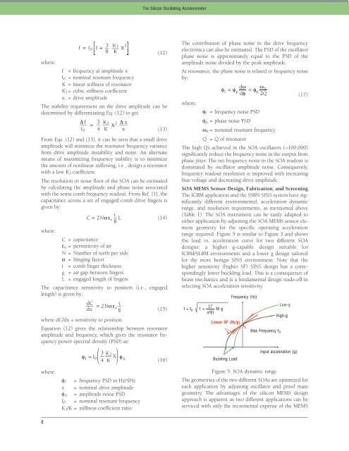
range required. Figure 5 is similar to Figure 3 and shows<br />
the load vs. acceleration curve for two different SOA<br />
designs: a higher g-capable design suitable for<br />
ICBM/SLBM environments and a lower g design tailored<br />
for the more benign SINS environment. Note that the<br />
higher sensitivity (higher SF) SINS design has a correspondingly<br />
lower buckling load. This is a consequence of<br />
beam mechanics and is a fundamental design trade-off in<br />
selecting SOA acceleration sensitivity.<br />
f = fo<br />
1 + M g<br />
π2EI L2 Linear SF (Hz/g)<br />
Buckling Load<br />
Frequency (Hz)<br />
Bias Frequency fo<br />
Low-g<br />
High-g<br />
Input acceleration (g)<br />
Figure 5. SOA dynamic range.<br />
The geometries of the two different SOAs are optimized for<br />
each application by adjusting oscillator and proof mass<br />
geometry. The advantages of the silicon MEMS design<br />
approach is apparent as two different applications can be<br />
serviced with only the incremental expense of the MEMS