LTC6945 - Ultralow Noise and Spurious 0.35GHz to 6GHz Integer-N ...
LTC6945 - Ultralow Noise and Spurious 0.35GHz to 6GHz Integer-N ...
LTC6945 - Ultralow Noise and Spurious 0.35GHz to 6GHz Integer-N ...

Create successful ePaper yourself
Turn your PDF publications into a flip-book with our unique Google optimized e-Paper software.
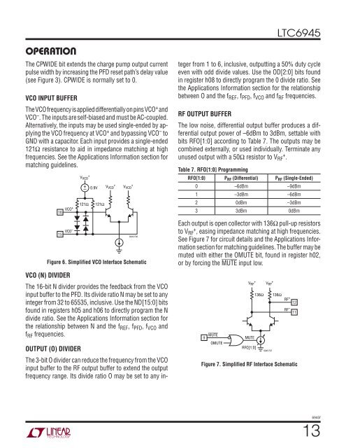
OPERATION<br />
The CPWIDE bit extends the charge pump output current<br />
pulse width by increasing the PFD reset path’s delay value<br />
(see Figure 3). CPWIDE is normally set <strong>to</strong> 0.<br />
VCO INPUT BUFFER<br />
The VCO frequency is applied differentially on pins VCO + <strong>and</strong><br />
VCO – . The inputs are self-biased <strong>and</strong> must be AC-coupled.<br />
Alternatively, the inputs may be used single-ended by applying<br />
the VCO frequency at VCO + <strong>and</strong> bypassing VCO – <strong>to</strong><br />
GND with a capaci<strong>to</strong>r. Each input provides a single-ended<br />
121Ω resistance <strong>to</strong> aid in impedance matching at high<br />
frequencies. See the Applications Information section for<br />
matching guidelines.<br />
16<br />
15<br />
VCO +<br />
VC0 –<br />
V VCO +<br />
+ –<br />
121Ω<br />
0.9V<br />
121Ω<br />
V VCO +<br />
V VCO +<br />
6945 F06<br />
Figure 6. Simplified VCO Interface Schematic<br />
VCO (N) DIVIDER<br />
The 16-bit N divider provides the feedback from the VCO<br />
input buffer <strong>to</strong> the PFD. Its divide ratio N may be set <strong>to</strong> any<br />
integer from 32 <strong>to</strong> 65535, inclusive. Use the ND[15:0] bits<br />
found in registers h05 <strong>and</strong> h06 <strong>to</strong> directly program the N<br />
divide ratio. See the Applications Information section for<br />
the relationship between N <strong>and</strong> the fREF , fPFD, fVCO <strong>and</strong><br />
fRF frequencies.<br />
OUTPUT (O) DIVIDER<br />
The 3-bit O divider can reduce the frequency from the VCO<br />
input buffer <strong>to</strong> the RF output buffer <strong>to</strong> extend the output<br />
frequency range. Its divide ratio O may be set <strong>to</strong> any in-<br />
Figure 7. Simplified RF Interface Schematic<br />
<strong>LTC6945</strong><br />
teger from 1 <strong>to</strong> 6, inclusive, outputting a 50% duty cycle<br />
even with odd divide values. Use the OD[2:0] bits found<br />
in register h08 <strong>to</strong> directly program the 0 divide ratio. See<br />
the Applications Information section for the relationship<br />
between O <strong>and</strong> the fREF , fPFD, fVCO <strong>and</strong> fRF frequencies.<br />
RF OUTPUT BUFFER<br />
The low noise, differential output buffer produces a differential<br />
output power of –6dBm <strong>to</strong> 3dBm, settable with<br />
bits RFO[1:0] according <strong>to</strong> Table 7. The outputs may be<br />
combined externally, or used individually. Terminate any<br />
unused output with a 50Ω resis<strong>to</strong>r <strong>to</strong> VRF + .<br />
Table 7. RFO[1:0] Programming<br />
RFO[1:0} PRF (Differential) PRF (Single-Ended)<br />
0 –6dBm –9dBm<br />
1 –3dBm –6dBm<br />
2 0dBm –3dBm<br />
3 3dBm 0dBm<br />
Each output is open collec<strong>to</strong>r with 136Ω pull-up resis<strong>to</strong>rs<br />
<strong>to</strong> VRF + , easing impedance matching at high frequencies.<br />
See Figure 7 for circuit details <strong>and</strong> the Applications Information<br />
section for matching guidelines. The buffer may be<br />
muted with either the OMUTE bit, found in register h02,<br />
or by forcing the MUTE input low.<br />
9<br />
OMUTE<br />
MUTE<br />
V RF +<br />
MUTE<br />
RFO[1:0]<br />
136Ω<br />
V RF +<br />
6945 F07<br />
RF<br />
12<br />
11<br />
+<br />
136Ω<br />
RF –<br />
6945f<br />
13