LTC6945 - Ultralow Noise and Spurious 0.35GHz to 6GHz Integer-N ...
LTC6945 - Ultralow Noise and Spurious 0.35GHz to 6GHz Integer-N ...
LTC6945 - Ultralow Noise and Spurious 0.35GHz to 6GHz Integer-N ...

Create successful ePaper yourself
Turn your PDF publications into a flip-book with our unique Google optimized e-Paper software.
APPLICATIONS INFORMATION<br />
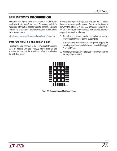
resistance (see Figure 22 for an example). See QFN Package<br />
Users Guide, page 8, on Linear Technology website’s<br />
Packaging Information page for specific recommendations<br />
concerning l<strong>and</strong> patterns <strong>and</strong> l<strong>and</strong> via solder masks. Links<br />
are provided below.<br />
http://www.linear.com/design<strong>to</strong>ols/packaging/index.jsp<br />
REFERENCE SIGNAL ROUTING AND SPURIOUS<br />
The charge pump operates at the PFD’s update frequency<br />
fPFD. The resultant output spurious energy is small <strong>and</strong><br />
is further reduced by the loop filter before it modulates<br />
the VCO frequency.<br />
6945 F22<br />
Figure 22. Example Exposed Pad L<strong>and</strong> Pattern<br />
<strong>LTC6945</strong><br />
However, improper PCB layout can degrade the <strong>LTC6945</strong>’s<br />
inherent spurious performance. Care must be taken <strong>to</strong><br />
prevent the reference signal fREF from coupling on<strong>to</strong> the<br />
VCO’s tune line, or in<strong>to</strong> other loop filter signals. Example<br />
suggestions are the following.<br />
1. Do not share power supply decoupling capaci<strong>to</strong>rs<br />
between same voltage power supply pins.<br />
2. Use separate ground vias for each power supply decoupling<br />
capaci<strong>to</strong>r, especially those connected <strong>to</strong> VREF + ,<br />
VCP + , <strong>and</strong> VVCO + .<br />
3. Physically separate the reference frequency signal from<br />
the loop filter <strong>and</strong> VCO.<br />
6945f<br />
25