LTC6945 - Ultralow Noise and Spurious 0.35GHz to 6GHz Integer-N ...
LTC6945 - Ultralow Noise and Spurious 0.35GHz to 6GHz Integer-N ...
LTC6945 - Ultralow Noise and Spurious 0.35GHz to 6GHz Integer-N ...

Create successful ePaper yourself
Turn your PDF publications into a flip-book with our unique Google optimized e-Paper software.
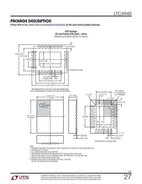
PACKAGE DESCRIPTION<br />
Please refer <strong>to</strong> http://www.linear.com/design<strong>to</strong>ols/packaging/ for the most recent package drawings.<br />
4.50 � 0.05<br />
3.10 � 0.05<br />
2.50 REF<br />
5.00 � 0.10<br />
(2 SIDES)<br />
2.65 � 0.05<br />
PIN 1<br />
TOP MARK<br />
(NOTE 6)<br />
3.65 � 0.05<br />
0.25 �0.05<br />
0.50 BSC<br />
3.50 REF<br />
4.10 � 0.05<br />
5.50 � 0.05<br />
RECOMMENDED SOLDER PAD PITCH AND DIMENSIONS<br />
APPLY SOLDER MASK TO AREAS THAT ARE NOT SOLDERED<br />
4.00 � 0.10<br />
(2 SIDES)<br />
UFD Package<br />
28-Lead Plastic QFN (4mm × 5mm)<br />
(Reference LTC DWG # 05-08-1712 Rev B)<br />
0.70 �0.05<br />
PACKAGE OUTLINE<br />
0.75 � 0.05<br />
3.50 REF<br />
0.200 REF<br />
0.00 – 0.05<br />
R = 0.05<br />
TYP<br />
NOTE:<br />
1. DRAWING PROPOSED TO BE MADE A JEDEC PACKAGE OUTLINE MO-220 VARIATION (WXXX-X).<br />
2. DRAWING NOT TO SCALE<br />
3. ALL DIMENSIONS ARE IN MILLIMETERS<br />
4. DIMENSIONS OF EXPOSED PAD ON BOTTOM OF PACKAGE DO NOT INCLUDE<br />
MOLD FLASH. MOLD FLASH, IF PRESENT, SHALL NOT EXCEED 0.15mm ON ANY SIDE<br />
5. EXPOSED PAD SHALL BE SOLDER PLATED<br />
6. SHADED AREA IS ONLY A REFERENCE FOR PIN 1 LOCATION<br />
ON THE TOP AND BOTTOM OF PACKAGE<br />
Information furnished by Linear Technology Corporation is believed <strong>to</strong> be accurate <strong>and</strong> reliable.<br />
However, no responsibility is assumed for its use. Linear Technology Corporation makes no representation<br />
that the interconnection of its circuits as described herein will not infringe on existing patent rights.<br />
BOTTOM VIEW—EXPOSED PAD<br />
<strong>LTC6945</strong><br />
2.50 REF<br />
R = 0.115<br />
TYP<br />
PIN 1 NOTCH<br />
R = 0.20 OR 0.35<br />
� 45� CHAMFER<br />
27 28<br />
3.65 � 0.10<br />
2.65 � 0.10<br />
0.40 � 0.10<br />
1<br />
2<br />
(UFD28) QFN 0506 REV B<br />
0.25 � 0.05<br />
0.50 BSC<br />
6945f<br />
27