LTC6945 - Ultralow Noise and Spurious 0.35GHz to 6GHz Integer-N ...
LTC6945 - Ultralow Noise and Spurious 0.35GHz to 6GHz Integer-N ...
LTC6945 - Ultralow Noise and Spurious 0.35GHz to 6GHz Integer-N ...

You also want an ePaper? Increase the reach of your titles
YUMPU automatically turns print PDFs into web optimized ePapers that Google loves.
OPERATION<br />
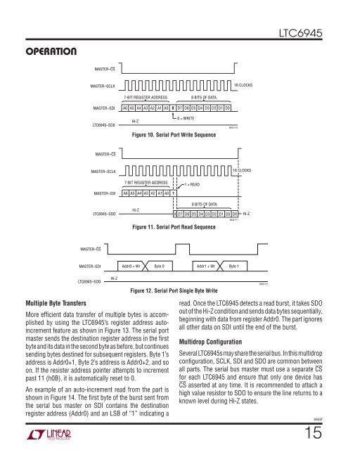
MASTER–CS<br />
MASTER–SCLK<br />
MASTER–CS<br />
MASTER–SDI<br />
<strong>LTC6945</strong>–SDO<br />
MASTER–SDI<br />
<strong>LTC6945</strong>–SD0<br />
MASTER–CS<br />
MASTER–SCLK<br />
MASTER–SDI<br />
<strong>LTC6945</strong>–SDO<br />
7-BIT REGISTER ADDRESS<br />
A6 A5 A4 A3 A2<br />
Multiple Byte Transfers<br />
More efficient data transfer of multiple bytes is accomplished<br />
by using the <strong>LTC6945</strong>’s register address au<strong>to</strong>increment<br />
feature as shown in Figure 13. The serial port<br />
master sends the destination register address in the first<br />
byte <strong>and</strong> its data in the second byte as before, but continues<br />
sending bytes destined for subsequent registers. Byte 1’s<br />
address is Addr0+1, Byte 2’s address is Addr0+2, <strong>and</strong> so<br />
on. If the resister address pointer attempts <strong>to</strong> increment<br />
past 11 (h0B), it is au<strong>to</strong>matically reset <strong>to</strong> 0.<br />
An example of an au<strong>to</strong>-increment read from the part is<br />
shown in Figure 14. The first byte of the burst sent from<br />
the serial bus master on SDI contains the destination<br />
register address (Addr0) <strong>and</strong> an LSB of “1” indicating a<br />
Hi-Z<br />
Hi-Z<br />
8 BITS OF DATA<br />
A1 A0 0 D7 D6 D5 D4 D3 D2 D1 D0<br />
0 = WRITE<br />
Figure 10. Serial Port Write Sequence<br />
7-BIT REGISTER ADDRESS<br />
A6 A5 A4 A3 A2<br />
Hi-Z<br />
Addr0 + Wr<br />
A1 A0 1<br />
1 = READ<br />
8 BITS OF DATA<br />
Figure 11. Serial Port Read Sequence<br />
Figure 12. Serial Port Single Byte Write<br />
6945 F10<br />
X D7 D6 D5 D4 D3 D2 D1 D0 DX<br />
6945 F11<br />
Byte 0 Addr1 + Wr Byte 1<br />
16 CLOCKS<br />
16 CLOCKS<br />
Hi-Z<br />
6945 F12<br />
<strong>LTC6945</strong><br />
read. Once the <strong>LTC6945</strong> detects a read burst, it takes SDO<br />
out of the Hi-Z condition <strong>and</strong> sends data bytes sequentially,<br />
beginning with data from register Addr0. The part ignores<br />
all other data on SDI until the end of the burst.<br />
Multidrop Configuration<br />
Several <strong>LTC6945</strong>s may share the serial bus. In this multidrop<br />
configuration, SCLK, SDI <strong>and</strong> SDO are common between<br />
all parts. The serial bus master must use a separate CS<br />
for each <strong>LTC6945</strong> <strong>and</strong> ensure that only one device has<br />
CS asserted at any time. It is recommended <strong>to</strong> attach a<br />
high value resis<strong>to</strong>r <strong>to</strong> SDO <strong>to</strong> ensure the line returns <strong>to</strong> a<br />
known level during Hi-Z states.<br />
6945f<br />
15