

A Low-Voltage SiGe BiCMOS 77-GHz Automotive Radar Chipset
A Low-Voltage SiGe BiCMOS 77-GHz Automotive Radar Chipset
A Low-Voltage SiGe BiCMOS 77-GHz Automotive Radar Chipset

Create successful ePaper yourself
Turn your PDF publications into a flip-book with our unique Google optimized e-Paper software.
NICOLSON et al.: LOW-VOLTAGE <strong>SiGe</strong> <strong>BiCMOS</strong> <strong>77</strong>-<strong>GHz</strong> AUTOMOTIVE RADAR CHIPSET 1093<br />
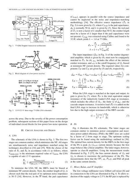
Fig. 1. <strong>77</strong>-<strong>GHz</strong> Doppler transceiver architecture.<br />
Fig. 2. Block diagram of a low-power receiver.<br />
Fig. 3. 1.8-V/2.5-V three-stage <strong>77</strong>-<strong>GHz</strong> LNA schematic.<br />
across the array. Due to the severity of the power consumption<br />
problem, subsequent sections of this paper focus on the design<br />
of individual circuit blocks for low-power low-noise operation.<br />
III. CIRCUIT ANALYSIS AND DESIGN<br />
A. LNA<br />
The schematic of the LNA is shown in Fig. 3. The first two<br />
stages are common emitter, which minimizes the NF. All stages<br />
are simultaneously noise and impedance matched using the<br />
techniques described in [34] and [35]. With the choice of the<br />
ratio of and in accordance with (1) as follows, where<br />
is the minimum required value of , the LNA<br />
is capable of sub-1.5 V operation.<br />
To minimize the LNA NF, the HBTs must be biased at<br />
minimum NF current density. Next, the emitter length of is<br />
chosen such that the real part of its optimum noise impedance<br />
is 50 [34]. However, in the -band, the pad capacitance<br />
(1)<br />
( ), appears in parallel with the source impedance and<br />
cannot be neglected in the noise and impedance-matching<br />
methodology [34]. The effective source impedance ( in<br />
Fig. 3) is now given by (2), where is the pad capacitance,<br />
is normally 50 , and is given by (3). Since the real part<br />
of is now a factor of smaller than 50 , the emitter length<br />
must be a factor of larger than if the pad capacitance were<br />
not present. was extracted using Calibre and found to be<br />
32 fF, which yields at <strong>77</strong> <strong>GHz</strong>.<br />
The input impedance ( in Fig. 3) of the emitter degenerated<br />
amplifier, which is given by (4), must now be conjugately<br />
matched to . In (4), includes the effect of the intrinsic<br />
emitter resistance, and is the cutoff frequency of biased<br />
at minimum NF current density. The required values for components<br />
and are given by (5) and (6), respectively.<br />
When the LNA stage is matched at the input and output, its<br />
gain is given by (7), where is the total equivalent output<br />
resistance of the inductively loaded LNA stage at resonance,<br />
which includes the effect of , the finite of , and the<br />
cascode output resistance. A resistive load ( ) is added on the<br />
final LNA stage to increase its bandwidth, which is otherwise<br />
low due to the high output resistance of the HBT cascode.<br />
B. PA<br />
Fig. 4 illustrates the PA schematic. The latter stages are<br />
common emitter to minimize power consumption and maximize<br />
power-added efficiency (PAE); the HBT sizes are scaled<br />
by a factor of 2 from stage to stage. The optimum scaling<br />
factor can be found using the methodology outlined in [36].<br />
The optimal bias current density for the HBTs in the first stage<br />
of the PA is peak current density because the first<br />
stage behaves like a linear amplifier. The latter stages, however,<br />
operate as class-B amplifiers. Using the measurement results<br />
illustrated in Fig. 5 [37], the bias current density of and<br />
is chosen to maximize the performance of the PA. The<br />
measurements show that the , , and PAE all peak<br />
at the same current density.<br />
C. Mixer, Balun, and IF Amplifier<br />
The low-voltage millimeter-wave Gilbert cell mixer [8] and<br />
its connection to the LNA are illustrated in Fig. 6. To allow reduction<br />
of the supply voltage to 2.5 V, the RF pair is replaced by<br />
(2)<br />
(3)<br />
(4)<br />
(5)<br />
(6)<br />
(7)


