

A Low-Voltage SiGe BiCMOS 77-GHz Automotive Radar Chipset
A Low-Voltage SiGe BiCMOS 77-GHz Automotive Radar Chipset
A Low-Voltage SiGe BiCMOS 77-GHz Automotive Radar Chipset

Create successful ePaper yourself
Turn your PDF publications into a flip-book with our unique Google optimized e-Paper software.
1096 IEEE TRANSACTIONS ON MICROWAVE THEORY AND TECHNIQUES, VOL. 56, NO. 5, MAY 2008<br />
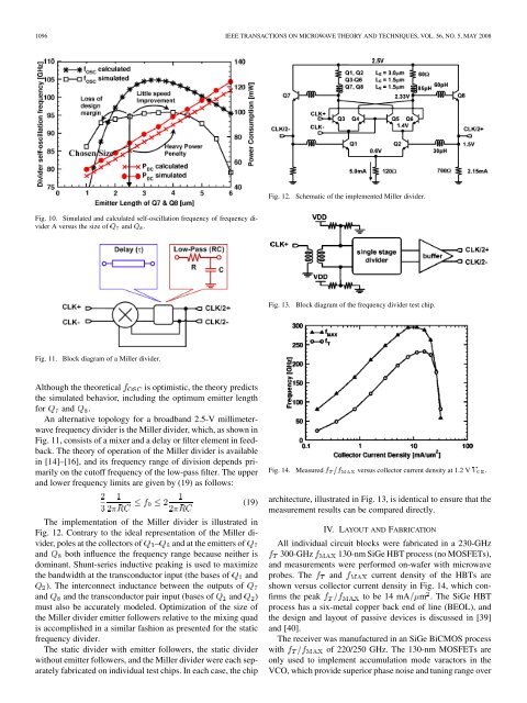
Fig. 10. Simulated and calculated self-oscillation frequency of frequency divider<br />
A versus the size of and .<br />
Fig. 11. Block diagram of a Miller divider.<br />
Although the theoretical is optimistic, the theory predicts<br />
the simulated behavior, including the optimum emitter length<br />
for and .<br />
An alternative topology for a broadband 2.5-V millimeterwave<br />
frequency divider is the Miller divider, which, as shown in<br />
Fig. 11, consists of a mixer and a delay or filter element in feedback.<br />
The theory of operation of the Miller divider is available<br />
in [14]–[16], and its frequency range of division depends primarily<br />
on the cutoff frequency of the low-pass filter. The upper<br />
and lower frequency limits are given by (19) as follows:<br />
(19)<br />
The implementation of the Miller divider is illustrated in<br />
Fig. 12. Contrary to the ideal representation of the Miller divider,<br />
poles at the collectors of – and at the emitters of<br />
and both influence the frequency range because neither is<br />
dominant. Shunt-series inductive peaking is used to maximize<br />
the bandwidth at the transconductor input (the bases of and<br />
). The interconnect inductance between the outputs of<br />
and and the transconductor pair input (bases of and )<br />
must also be accurately modeled. Optimization of the size of<br />
the Miller divider emitter followers relative to the mixing quad<br />
is accomplished in a similar fashion as presented for the static<br />
frequency divider.<br />
The static divider with emitter followers, the static divider<br />
without emitter followers, and the Miller divider were each separately<br />
fabricated on individual test chips. In each case, the chip<br />
Fig. 12. Schematic of the implemented Miller divider.<br />
Fig. 13. Block diagram of the frequency divider test chip.<br />
Fig. 14. Measured � a� versus collector current density at 1.2 V † .<br />
architecture, illustrated in Fig. 13, is identical to ensure that the<br />
measurement results can be compared directly.<br />
IV. LAYOUT AND FABRICATION<br />
All individual circuit blocks were fabricated in a 230-<strong>GHz</strong><br />
300-<strong>GHz</strong> 130-nm <strong>SiGe</strong> HBT process (no MOSFETs),<br />
and measurements were performed on-wafer with microwave<br />
probes. The and current density of the HBTs are<br />
shown versus collector current density in Fig. 14, which confirms<br />
the peak to be 14 mA m . The <strong>SiGe</strong> HBT<br />
process has a six-metal copper back end of line (BEOL), and<br />
the design and layout of passive devices is discussed in [39]<br />
and [40].<br />
The receiver was manufactured in an <strong>SiGe</strong> <strong>BiCMOS</strong> process<br />
with of 220/250 <strong>GHz</strong>. The 130-nm MOSFETs are<br />
only used to implement accumulation mode varactors in the<br />
VCO, which provide superior phase noise and tuning range over


