

A Low-Voltage SiGe BiCMOS 77-GHz Automotive Radar Chipset
A Low-Voltage SiGe BiCMOS 77-GHz Automotive Radar Chipset
A Low-Voltage SiGe BiCMOS 77-GHz Automotive Radar Chipset

Create successful ePaper yourself
Turn your PDF publications into a flip-book with our unique Google optimized e-Paper software.
NICOLSON et al.: LOW-VOLTAGE <strong>SiGe</strong> <strong>BiCMOS</strong> <strong>77</strong>-<strong>GHz</strong> AUTOMOTIVE RADAR CHIPSET 1097<br />
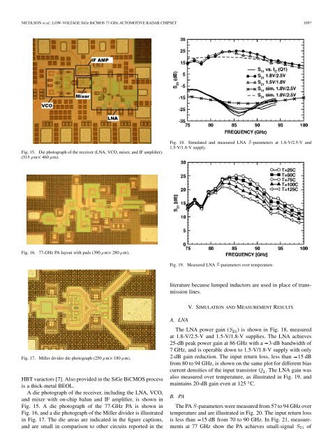
Fig. 15. Die photograph of the receiver (LNA, VCO, mixer, and IF amplifier).<br />
(515 "m2 460 "m).<br />
Fig. 16. <strong>77</strong>-<strong>GHz</strong> PA layout with pads (390 "m2 280 "m).<br />
Fig. 17. Miller divider die photograph (250 "m2 180 "m).<br />
HBT varactors [7]. Also provided in the <strong>SiGe</strong> <strong>BiCMOS</strong> process<br />
is a thick-metal BEOL.<br />
A die photograph of the receiver, including the LNA, VCO,<br />
and mixer with on-chip balun and IF amplifier, is shown in<br />
Fig. 15. A die photograph of the <strong>77</strong>-<strong>GHz</strong> PA is shown in<br />
Fig. 16, and a die photograph of the Miller divider is illustrated<br />
in Fig. 17. The die areas are indicated in the figure captions,<br />
and are small in comparison to other circuits reported in the<br />
Fig. 18. Simulated and measured LNA ƒ-parameters at 1.8-V/2.5-V and<br />
1.5-V/1.8-V supply.<br />
Fig. 19. Measured LNA ƒ-parameters over temperature.<br />
literature because lumped inductors are used in place of transmission<br />
lines.<br />
V. SIMULATION AND MEASUREMENT RESULTS<br />
A. LNA<br />
The LNA power gain ( ) is shown in Fig. 18, measured<br />
at 1.8-V/2.5-V and 1.5-V/1.8-V supplies. The LNA achieves<br />
25-dB peak power gain at 86 <strong>GHz</strong> with a 3-dB bandwidth of<br />
7 <strong>GHz</strong>, and is operable down to 1.5-V/1.8-V supply with only<br />
2-dB gain reduction. The input return loss, less than 15 dB<br />
from 80 to 94 <strong>GHz</strong>, is shown on the same plot for different bias<br />
current densities of the input transistor . The LNA gain was<br />
also measured over temperature, as illustrated in Fig. 19, and<br />
maintains 20-dB gain even at 125 C.<br />
B. PA<br />
The PA -parameters were measured from 57 to 94 <strong>GHz</strong> over<br />
temperature and are illustrated in Fig. 20. The input return loss<br />
is less than 15 dB from 70 to 90 <strong>GHz</strong>. In Fig. 21, measurements<br />
at <strong>77</strong> <strong>GHz</strong> show the PA achieves small-signal of


