

A Low-Voltage SiGe BiCMOS 77-GHz Automotive Radar Chipset
A Low-Voltage SiGe BiCMOS 77-GHz Automotive Radar Chipset
A Low-Voltage SiGe BiCMOS 77-GHz Automotive Radar Chipset

You also want an ePaper? Increase the reach of your titles
YUMPU automatically turns print PDFs into web optimized ePapers that Google loves.
1094 IEEE TRANSACTIONS ON MICROWAVE THEORY AND TECHNIQUES, VOL. 56, NO. 5, MAY 2008<br />
Fig. 4. 1.8-V/2.5-V <strong>77</strong>-<strong>GHz</strong> three-stage PA schematic.<br />
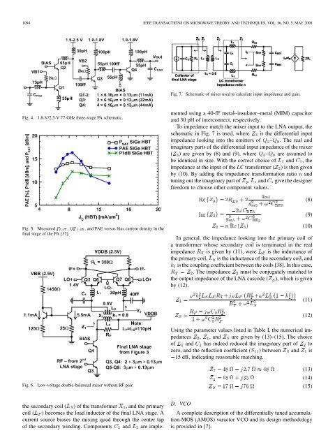
Fig. 5. Measured € , y€ , and PAE versus bias current density in the<br />
final stage of the PA [37].<br />
Fig. 6. <strong>Low</strong>-voltage double-balanced mixer without RF pair.<br />
the secondary coil ( ) of the transformer , and the primary<br />
coil ( ) becomes the load inductor of the final LNA stage. A<br />
current source biases the mixing quad through the center tap<br />
of the secondary winding. Components and are imple-<br />
Fig. 7. Schematic of mixer used to calculate input impedance and gain.<br />
mented using a 40-fF metal–insulator–metal (MIM) capacitor<br />
and 30 pH of interconnect, respectively.<br />
To impedance match the mixer input to the LNA output, the<br />
schematic in Fig. 7 is used, where is the differential input<br />
impedance looking into the emitters of – . The real and<br />
imaginary parts of the differential input impedance of the mixer<br />
( ) are given by (8) and (9), where – are assumed to<br />
be identical in size. With the correct choice of and , the<br />
impedance at the input of the LC transformer ( ) is then given<br />
by (10). By adding the impedance transformation ratio and<br />
tuning out the imaginary part of , and give the designer<br />
freedom to choose other component values.<br />
(8)<br />
(9)<br />
(10)<br />
In general, the impedance looking into the primary coil of<br />
a transformer whose secondary coil is terminated in the real<br />
impedance is given by (11), were is the inductance of<br />
the primary coil, is the inductance of the secondary coil, and<br />
is the coupling coefficient between the coils [38]. In this case,<br />
. The impedance must be conjugately matched to<br />
the output impedance of the LNA cascode ( ), which is given<br />
by (12).<br />
(11)<br />
(12)<br />
Using the parameter values listed in Table I, the numerical impedances<br />
, , and are given by (13)–(15). The choice<br />
of and has indeed reduced the imaginary part of to<br />
zero, and the reflection coefficient ( ) between and is<br />
15 dB, indicating reasonable matching.<br />
(13)<br />
(14)<br />
(15)<br />
D. VCO<br />
A complete description of the differentially tuned accumulation-MOS<br />
(AMOS) varactor VCO and its design methodology<br />
is provided in [7].


