Texas Journal of Microscopy - Texas Society for Microscopy
Texas Journal of Microscopy - Texas Society for Microscopy
Texas Journal of Microscopy - Texas Society for Microscopy

Create successful ePaper yourself
Turn your PDF publications into a flip-book with our unique Google optimized e-Paper software.
Electrical failures <strong>of</strong> an assembled board led to<br />
an investigation into root failure cause. In-circuit<br />
testing identified electrical opens at Ball Grid Array<br />
(BGA) solder bumps to the Printed Wire Board<br />
(PWB) interface. Scanning Electron <strong>Microscopy</strong><br />
(SEM), Energy Dispersive Spectroscopy (EDS),<br />
optical inspection and Fourier Trans<strong>for</strong>m Infrared<br />
were used to investigate this failure.<br />
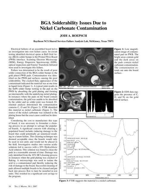
Failure was determined to be the result <strong>of</strong> poor<br />
solder connection <strong>of</strong> the BGA solder bumps to the<br />
gold plated PWB pads. Contamination was identified<br />
on the PWB pad surfaces causing the poor<br />
solderability. The cracked flaky appearance <strong>of</strong> the<br />
contaminant indicated the material was at one time<br />
in liquid <strong>for</strong>m (Figure ). A typical joint results in<br />
the SnPb solder bump wetting to the pad on the<br />
PWB by absorbing the gold plating and <strong>for</strong>ming<br />
an intermetallic with the underlying nickel plating.<br />
In instances where the pads on the board contain<br />
contamination, the gold was unable to be absorbed<br />
by the solder and no solder joint was <strong>for</strong>med. Elemental<br />
analysis determined the contamination<br />
contains C, O and Ni (Figure 2). FTIR identified<br />
this material as nickel carbonate (Figure 3). The<br />
source <strong>of</strong> the nickel carbonate was isolated to the<br />
plating house but the exact cause could not be identified.<br />
Considering the cost to manufacture this type<br />
<strong>of</strong> board, it was necessary to <strong>for</strong>mulate a cleaning<br />
process in an attempt to salvage the populated<br />
boards. A significant concern with cleaning a<br />
populated board includes inducing damage to the<br />
board that could potentially go unnoticed resulting<br />
in a latent failure. This cleaning technique was<br />
deemed acceptable since the boards would only<br />
be used in test units and would not be placed in<br />
the field. Investigative studies into various acidic<br />
solutions led to success with a 0% Hydrochloric<br />
Acid solution. This solution was found to clean the<br />
pads in a reasonable amount <strong>of</strong> time. Damage was<br />
only identified from the 0% HCl cleaning process<br />
in instances when the gold plating was cracked or<br />
flaking. A microsyringe was used to isolate the<br />
acid to a contaminated pad thereby reducing the<br />
risk <strong>of</strong> damage to the board. Successful cleaning <strong>of</strong><br />
pads allowed multiple boards to be cleaned and put<br />
back into process flow to later be installed in test<br />
units. This resulted in a significant cost savings to<br />
the program.<br />
6 Tex. J. Micros. 38: , 2007<br />
BGA Solderability Issues Due to<br />
Nickel Carbonate Contamination<br />
JODI A. ROEPSCH<br />
Raytheon NCS Shared Services Failure Analysis Lab, McKinney, <strong>Texas</strong> 75071<br />
Figure 3: FTIR suggests the material is a nickel carbonate.<br />
Figure 1: Low magnification<br />
image <strong>of</strong> contaminated<br />
pad on PWB. The<br />
bright areas contain gold<br />
and the dark areas on<br />
the pads contain nickel<br />
carbonate contamination.<br />
The contamination extends<br />
out onto the board<br />
surface.<br />
Figure 2: EDS data suggests<br />
the presence <strong>of</strong> C,<br />
O, and Ni on the gold<br />
plated surface.