NXP 80C552, 83/87C552, P80C562, P83C562 Family Overview - Keil
NXP 80C552, 83/87C552, P80C562, P83C562 Family Overview - Keil
NXP 80C552, 83/87C552, P80C562, P83C562 Family Overview - Keil

Create successful ePaper yourself
Turn your PDF publications into a flip-book with our unique Google optimized e-Paper software.
Philips Semiconductors<br />
80C51 <strong>Family</strong> Derivatives 8XC552/562 overview<br />
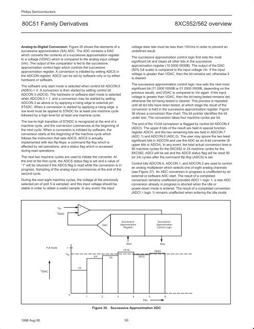
Analog-to-Digital Conversion: Figure 35 shows the elements of a<br />
successive approximation (SA) ADC. The ADC contains a DAC<br />
which converts the contents of a successive approximation register<br />
to a voltage (VDAC) which is compared to the analog input voltage<br />
(Vin). The output of the comparator is fed to the successive<br />
approximation control logic which controls the successive<br />
approximation register. A conversion is initiated by setting ADCS in<br />
the ADCON register. ADCS can be set by software only or by either<br />
hardware or software.<br />
The software only start mode is selected when control bit ADCON.5<br />
(ADEX) = 0. A conversion is then started by setting control bit<br />
ADCON.3 (ADCS). The hardware or software start mode is selected<br />
when ADCON.5 = 1, and a conversion may be started by setting<br />
ADCON.3 as above or by applying a rising edge to external pin<br />
STADC. When a conversion is started by applying a rising edge, a<br />
low level must be applied to STADC for at least one machine cycle<br />
followed by a high level for at least one machine cycle.<br />
The low-to-high transition of STADC is recognized at the end of a<br />
machine cycle, and the conversion commences at the beginning of<br />
the next cycle. When a conversion is initiated by software, the<br />
conversion starts at the beginning of the machine cycle which<br />
follows the instruction that sets ADCS. ADCS is actually<br />
implemented with two flip-flops: a command flip-flop which is<br />
affected by set operations, and a status flag which is accessed<br />
during read operations.<br />
The next two machine cycles are used to initiate the converter. At<br />
the end of the first cycle, the ADCS status flag is set and a value of<br />
“1” will be returned if the ADCS flag is read while the conversion is in<br />
progress. Sampling of the analog input commences at the end of the<br />
second cycle.<br />
During the next eight machine cycles, the voltage at the previously<br />
selected pin of port 5 is sampled, and this input voltage should be<br />
stable in order to obtain a useful sample. In any event, the input<br />
V DAC<br />
V in<br />
V DAC<br />
Full Scale 1<br />
V in<br />
0<br />
Successive<br />
Approximation<br />
Register<br />
1996 Aug 06 50<br />
+<br />
–<br />
1/2<br />
3/4<br />
DAC<br />
7/8<br />
15/16<br />
voltage slew rate must be less than 10V/ms in order to prevent an<br />
undefined result.<br />
The successive approximation control logic first sets the most<br />
significant bit and clears all other bits in the successive<br />
approximation register (10 0000 0000B). The output of the DAC<br />
(50% full scale) is compared to the input voltage Vin. If the input<br />
voltage is greater than VDAC, then the bit remains set; otherwise it<br />
is cleared.<br />
The successive approximation control logic now sets the next most<br />
significant bit (11 0000 0000B or 01 0000 0000B, depending on the<br />
previous result), and VDAC is compared to Vin again. If the input<br />
voltage is greater than VDAC, then the bit being tested remains set;<br />
otherwise the bit being tested is cleared. This process is repeated<br />
until all ten bits have been tested, at which stage the result of the<br />
conversion is held in the successive approximation register. Figure<br />
36 shows a conversion flow chart. The bit pointer identifies the bit<br />
under test. The conversion takes four machine cycles per bit.<br />
The end of the 10-bit conversion is flagged by control bit ADCON.4<br />
(ADCI). The upper 8 bits of the result are held in special function<br />
register ADCH, and the two remaining bits are held in ADCON.7<br />
(ADC.1) and ADCON.6 (ADC.0). The user may ignore the two least<br />
significant bits in ADCON and use the ADC as an 8-bit converter (8<br />
upper bits in ADCH). In any event, the total actual conversion time is<br />
50 machine cycles for the 8XC552 or 24 machine cycles for the<br />
8XC562. ADCI will be set and the ADCS status flag will be reset 50<br />
(or 24) cycles after the command flip-flop (ADCS) is set.<br />
Control bits ADCON.0, ADCON.1, and ADCON.2 are used to control<br />
an analog multiplexer which selects one of eight analog channels<br />
(see Figure 37). An ADC conversion in progress is unaffected by an<br />
external or software ADC start. The result of a completed<br />
conversion remains unaffected provided ADCI = logic 1; a new ADC<br />
conversion already in progress is aborted when the idle or<br />
power-down mode is entered. The result of a completed conversion<br />
(ADCI = logic 1) remains unaffected when entering the idle mode.<br />
Successive<br />
Approximation<br />
Control Logic<br />
Start Stop<br />
29/32<br />
59/64<br />
1 2 3 4 5 6<br />
t/tau<br />
Figure 35. Successive Approximation ADC