NXP 80C552, 83/87C552, P80C562, P83C562 Family Overview - Keil
NXP 80C552, 83/87C552, P80C562, P83C562 Family Overview - Keil
NXP 80C552, 83/87C552, P80C562, P83C562 Family Overview - Keil

You also want an ePaper? Increase the reach of your titles
YUMPU automatically turns print PDFs into web optimized ePapers that Google loves.
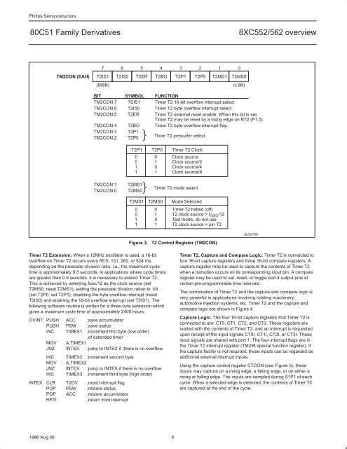
Philips Semiconductors<br />
80C51 <strong>Family</strong> Derivatives 8XC552/562 overview<br />
TM2CON (EAH)<br />
T2IS1<br />
T2IS0<br />
T2ER<br />
1996 Aug 06 6<br />
7<br />
(MSB)<br />
T2MS0<br />
BIT SYMBOL FUNCTION<br />
TM2CON.7 TSIS1 Timer T2 16-bit overflow interrupt select<br />
TM2CON.6 T2IS0 Timer T2 byte overflow interrupt select<br />
TM2CON.5 T2ER Timer T2 external reset enable. When this bit is set,<br />
Timer T2 may be reset by a rising edge on RT2 (P1.5).<br />
TM2CON.4 T2BO Timer T2 byte overflow interrupt flag<br />
TM2CON.3<br />
TM2CON.2<br />
T2P1<br />
T2P0<br />
Timer T2 prescaler select<br />
TM2CON.1 T2MS1<br />
TM2CON.0 T2MS0<br />
6<br />
5<br />
4<br />
T2BO<br />
3<br />
T2P1<br />
2<br />
T2P0<br />
T2P1 T2P0 Timer T2 Clock<br />
0 0 Clock source<br />
0 1 Clock source/2<br />
1 0 Clock source/4<br />
1 1 Clock source/8<br />
Timer T2 mode select<br />
T2MS1 T2MS0 Mode Selected<br />
Timer T2 Extension: When a 12MHz oscillator is used, a 16-bit<br />
overflow on Timer T2 occurs every 65.5, 131, 262, or 524 ms,<br />
depending on the prescaler division ratio; i.e., the maximum cycle<br />
time is approximately 0.5 seconds. In applications where cycle times<br />
are greater than 0.5 seconds, it is necessary to extend Timer T2.<br />
This is achieved by selecting fosc/12 as the clock source (set<br />
T2MS0, reset T2MS1), setting the prescaler division ration to 1/8<br />
(set T2P0, set T2P1), disabling the byte overflow interrupt (reset<br />
T2IS0) and enabling the 16-bit overflow interrupt (set T2IS1). The<br />
following software routine is written for a three-byte extension which<br />
gives a maximum cycle time of approximately 2400 hours.<br />
OVINT: PUSH ACC ;save accumulator<br />
PUSH PSW ;save status<br />
INC TIMEX1 ;increment first byte (low order)<br />
;of extended timer<br />
MOV A,TIMEX1<br />
JNZ INTEX ;jump to INTEX if ;there is no overflow<br />
INC TIMEX2 ;increment second byte<br />
MOV A,TIMEX2<br />
JNZ INTEX ;jump to INTEX if there is no overflow<br />
INC TIMEX3 ;increment third byte (high order)<br />
INTEX: CLR T2OV ;reset interrupt flag<br />
POP PSW ;restore status<br />
POP ACC ;restore accumulator<br />
RETI ;return from interrupt<br />
1<br />
T2MS1<br />
0 0 Timer T2 halted (off)<br />
0 1 T2 clock source = f OSC/12<br />
1 0 Test mode; do not use<br />
1 1 T2 clock source = pin T2<br />
Figure 3. T2 Control Register (TM2CON)<br />
0<br />
(LSB)<br />
SU00756<br />
Timer T2, Capture and Compare Logic: Timer T2 is connected to<br />
four 16-bit capture registers and three 16-bit compare registers. A<br />
capture register may be used to capture the contents of Timer T2<br />
when a transition occurs on its corresponding input pin. A compare<br />
register may be used to set, reset, or toggle port 4 output pins at<br />
certain pre-programmable time intervals.<br />
The combination of Timer T2 and the capture and compare logic is<br />
very powerful in applications involving rotating machinery,<br />
automotive injection systems, etc. Timer T2 and the capture and<br />
compare logic are shown in Figure 4.<br />
Capture Logic: The four 16-bit capture registers that Timer T2 is<br />
connected to are: CT0, CT1, CT2, and CT3. These registers are<br />
loaded with the contents of Timer T2, and an interrupt is requested<br />
upon receipt of the input signals CT0I, CT1I, CT2I, or CT3I. These<br />
input signals are shared with port 1. The four interrupt flags are in<br />
the Timer T2 interrupt register (TM2IR special function register). If<br />
the capture facility is not required, these inputs can be regarded as<br />
additional external interrupt inputs.<br />
Using the capture control register CTCON (see Figure 5), these<br />
inputs may capture on a rising edge, a falling edge, or on either a<br />
rising or falling edge. The inputs are sampled during S1P1 of each<br />
cycle. When a selected edge is detected, the contents of Timer T2<br />
are captured at the end of the cycle.