6-2019
Fachzeitschrift für Hochfrequenz- und Mikrowellentechnik
Fachzeitschrift für Hochfrequenz- und Mikrowellentechnik

Sie wollen auch ein ePaper? Erhöhen Sie die Reichweite Ihrer Titel.
YUMPU macht aus Druck-PDFs automatisch weboptimierte ePaper, die Google liebt.
RF & Wireless<br />
Figure 2: Allocation of the intra-band and inter-band carriers (image courtesy of Qorvo)<br />
Figure 3: BAW resonator (right) and BAW cross-section (left) of a Van Dyke<br />
model<br />
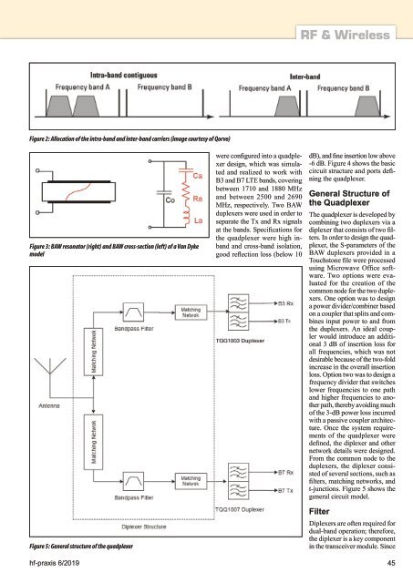
Figure 5: General structure of the quadplexer<br />
were configured into a quadplexer<br />
design, which was simulated<br />
and realized to work with<br />
B3 and B7 LTE bands, covering<br />
between 1710 and 1880 MHz<br />
and between 2500 and 2690<br />
MHz, respectively. Two BAW<br />
duplexers were used in order to<br />
separate the Tx and Rx signals<br />
at the bands. Specifications for<br />
the quadplexer were high inband<br />
and cross-band isolation,<br />
good reflection loss (below 10<br />
dB), and fine insertion low above<br />
-6 dB. Figure 4 shows the basic<br />
circuit structure and ports defining<br />
the quadplexer.<br />
General Structure of<br />
the Quadplexer<br />
The quadplexer is developed by<br />
combining two duplexers via a<br />
diplexer that consists of two filters.<br />
In order to design the quadplexer,<br />
the S-parameters of the<br />
BAW duplexers provided in a<br />
Touchstone file were processed<br />
using Microwave Office software.<br />
Two options were evaluated<br />
for the creation of the<br />
common node for the two duplexers.<br />
One option was to design<br />
a power divider/combiner based<br />
on a coupler that splits and combines<br />
input power to and from<br />
the duplexers. An ideal coupler<br />
would introduce an additional<br />
3 dB of insertion loss for<br />
all frequencies, which was not<br />
desirable because of the two-fold<br />
increase in the overall insertion<br />
loss. Option two was to design a<br />
frequency divider that switches<br />
lower frequencies to one path<br />
and higher frequencies to another<br />
path, thereby avoiding much<br />
of the 3-dB power loss incurred<br />
with a passive coupler architecture.<br />
Once the system requirements<br />
of the quadplexer were<br />
defined, the diplexer and other<br />
network details were designed.<br />
From the common node to the<br />
duplexers, the diplexer consisted<br />
of several sections, such as<br />
filters, matching networks, and<br />
t-junctions. Figure 5 shows the<br />
general circuit model.<br />
Filter<br />
Diplexers are often required for<br />
dual-band operation; therefore,<br />
the diplexer is a key component<br />
in the transceiver module. Since<br />
hf-praxis 6/<strong>2019</strong> 45