

Automotive Innovators Hit High Gear in - Xilinx
Automotive Innovators Hit High Gear in - Xilinx
Automotive Innovators Hit High Gear in - Xilinx

You also want an ePaper? Increase the reach of your titles
YUMPU automatically turns print PDFs into web optimized ePapers that Google loves.
XCELLENCE IN NEW APPLICATIONS<br />
The Virtex-5’s pre-bit deskew capability, which is built <strong>in</strong>to all<br />
I/O blocks (IODELAY primitive), helped us to meet setup-and-hold<br />
requirements at <strong>in</strong>put and output stage.<br />
implemented <strong>in</strong> RTL logic with Xil<strong>in</strong>x<br />
tools. We recommend us<strong>in</strong>g standard RTL<br />
logic to implement the multiply-accumulate,<br />
ADDR and multiplier. Include the<br />
design constra<strong>in</strong>ts dur<strong>in</strong>g synthesis and<br />
placement and rout<strong>in</strong>g.<br />
For IP <strong>in</strong>tegration, be sure to have a separate<br />
clock-reset module for each FPGA.<br />
The asynchronous reset must be synchronous<br />
with each and every clock, both global<br />
and regional. Internally, the reset signal is<br />
asserted asynchronously and deasserted<br />
synchronously with respect to specific<br />
clocks, and its output is applied to the specific<br />
module to which the clock belongs.<br />
Make sure you have connected all the global<br />
<strong>in</strong>put clocks to the PLL/DCM core generated<br />
by CoreGen.<br />
Also, be sure you’ve connected the<br />
regional clock to BUFR/BUFIO. In addition,<br />
to keep your placement-and-rout<strong>in</strong>g<br />
tool from us<strong>in</strong>g unnecessary rout<strong>in</strong>g<br />
resources, make sure you generate only the<br />
necessary reset signals. You need to ensure<br />
that PLL/DCM lock conditions are<br />
brought to external p<strong>in</strong>s or to the configuration<br />
register. In our case, we only connected<br />
the 200-MHz system clock PLL<br />
lock to the I/O p<strong>in</strong>s.<br />
Def<strong>in</strong>ition of the IOB (<strong>in</strong>put, output or<br />
both <strong>in</strong>put and output) synthesis and mapp<strong>in</strong>g<br />
constra<strong>in</strong>ts must be part of the<br />
FPGA’s top RTL module. We <strong>in</strong>stantiated<br />
the topmost module of core logic <strong>in</strong>side the<br />
FPGA’s top module. It must communicate<br />
with the external <strong>in</strong>terface via these IOB<br />
def<strong>in</strong>itions only.<br />
IOB def<strong>in</strong>itions consist of IBUF,<br />
OBUF, IBUFDS, OBUFDS and the like.<br />
Each <strong>in</strong> turn consists of supported userdef<strong>in</strong>ed<br />
parameters for IO_STANDARD<br />
(LVTTL, LVCMOS, etc). We used the<br />
<strong>in</strong>stance def<strong>in</strong>ition of the above to map<br />
external I/O signals with the topmost RTL<br />
module signals.<br />
S<strong>in</strong>ce we were design<strong>in</strong>g with highspeed<br />
source-synchronous <strong>in</strong>puts and out-<br />
puts, the Virtex-5’s pre-bit deskew capability,<br />
which is built <strong>in</strong>to all I/O blocks<br />
(IODELAY primitive), helped us to meet<br />
setup-and-hold requirements at <strong>in</strong>put and<br />
output stage. For source-synchronous<br />
<strong>in</strong>puts, the source-synchronous clock uses<br />
BUFIO or BUFR, and it <strong>in</strong>troduces additional<br />
delay. To compensate for this delay,<br />
we drove data and clock <strong>in</strong>puts via an<br />
IODELAY <strong>in</strong>stance that we configured <strong>in</strong><br />
<strong>in</strong>put delay mode with known delay<br />
counts. Chang<strong>in</strong>g the delay count value<br />
helped us meet tim<strong>in</strong>g requirements at the<br />
<strong>in</strong>put stage.<br />
Similarly at the output stage, as synchronous<br />
clock signals are driven with<br />
data, we needed to make sure that data<br />
and clock signals were driven so as to meet<br />
the setup-and-hold of an FPGA or ASIC<br />
at the other end. We used IODELAY<br />
<strong>in</strong>stances configured <strong>in</strong> an output delay<br />
mode with a known delay count value for<br />
both clock and data outputs. The IODE-<br />
LAY needs an IODELAYCTRL primitive<br />
<strong>in</strong>stance at the top of the FPGA. The 200-<br />
MHz <strong>in</strong>put clock<strong>in</strong>g to the IODELAY-<br />
CTRL <strong>in</strong>stance creates a delay count<br />
precision of 70 ps on IODELAY.<br />
Video ch1_data<br />
Video ch1_clk<br />
Tim<strong>in</strong>g Consideration<br />
and Constra<strong>in</strong>ts Def<strong>in</strong>itions<br />
After generat<strong>in</strong>g and implement<strong>in</strong>g the IP,<br />
the next step was to perform tim<strong>in</strong>g. We<br />
constra<strong>in</strong>ed all the <strong>in</strong>put clocks for period,<br />
jitter and <strong>in</strong>put offset delays, and set all output<br />
delays with respect to the source clock<br />
and <strong>in</strong>put-to-output delay. We then created<br />
the tim<strong>in</strong>g and placement constra<strong>in</strong>ts <strong>in</strong><br />
Xil<strong>in</strong>x User Constra<strong>in</strong>t Files (UCFs).<br />
We constra<strong>in</strong>ed all the <strong>in</strong>put clocks to<br />
specific frequencies and also def<strong>in</strong>ed the<br />
jitter <strong>in</strong>put us<strong>in</strong>g the follow<strong>in</strong>g UCF code:<br />
NET “i_clk_200_s”<br />
TNM_NET = “IN_200_CLKGRP”;<br />
TIMESPEC “IN_200_CLKGRP”<br />
= PERIOD 5 ns HIGH 50%<br />
INPUT_JITTER 0.1 ns<br />
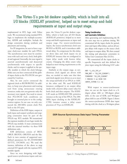
With respect to source-synchronous<br />
data, we can set the <strong>in</strong>put clock to a 0degree<br />
phase shift or 180-degree phase<br />
shift, <strong>in</strong> the case of SDR, and 90-degree<br />
phase shift <strong>in</strong> case of DDR. Figure 2 shows<br />
the source-synchronous DDR data <strong>in</strong>put<br />
tim<strong>in</strong>g with the clock at a 90-degree phase<br />
DDR Source Synchronous Data Input Tim<strong>in</strong>g Parameter<br />
38 Xcell Journal Fourth Quarter 2008<br />
tv<br />
DATA_P DATA_N<br />
ts_p th<br />
ts_n<br />
tclk<br />
Figure 2 – Tim<strong>in</strong>g Diagram of DDR Inputs


