

C8051F326/7 - Silicon Labs
C8051F326/7 - Silicon Labs
C8051F326/7 - Silicon Labs

You also want an ePaper? Increase the reach of your titles
YUMPU automatically turns print PDFs into web optimized ePapers that Google loves.
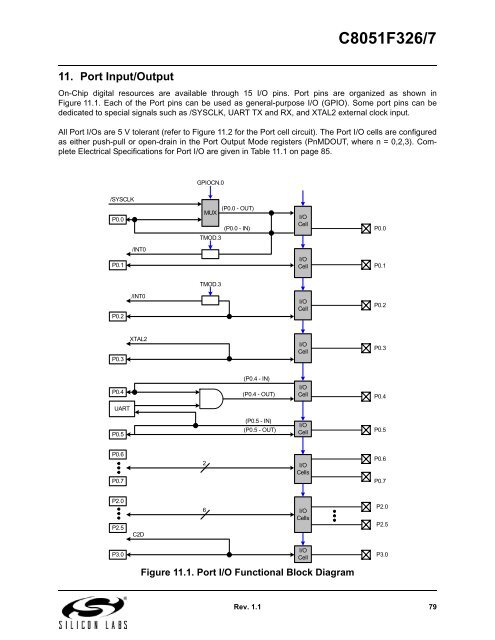
11. Port Input/Output<br />
<strong>C8051F326</strong>/7<br />
On-Chip digital resources are available through 15 I/O pins. Port pins are organized as shown in<br />
Figure 11.1. Each of the Port pins can be used as general-purpose I/O (GPIO). Some port pins can be<br />
dedicated to special signals such as /SYSCLK, UART TX and RX, and XTAL2 external clock input.<br />
All Port I/Os are 5 V tolerant (refer to Figure 11.2 for the Port cell circuit). The Port I/O cells are configured<br />
as either push-pull or open-drain in the Port Output Mode registers (PnMDOUT, where n = 0,2,3). Complete<br />
Electrical Specifications for Port I/O are given in Table 11.1 on page 85.<br />
/SYSCLK<br />
P0.0<br />
P0.1<br />
P0.2<br />
P0.3<br />
P0.4<br />
UART<br />
P0.5<br />
P0.6<br />
P0.7<br />
P2.0<br />
P2.5<br />
P3.0<br />
/INT0<br />
/INT0<br />
XTAL2<br />
C2D<br />
GPIOCN.0<br />
MUX<br />
TMOD.3<br />
TMOD.3<br />
2<br />
6<br />
(P0.0 - OUT)<br />
(P0.0 - IN)<br />
(P0.4 - IN)<br />
(P0.4 - OUT)<br />
(P0.5 - IN)<br />
(P0.5 - OUT)<br />
I/O<br />
Cell<br />
I/O<br />
Cell<br />
I/O<br />
Cell<br />
I/O<br />
Cell<br />
I/O<br />
Cell<br />
I/O<br />
Cell<br />
I/O<br />
Cells<br />
I/O<br />
Cells<br />
I/O<br />
Cell<br />
Figure 11.1. Port I/O Functional Block Diagram<br />
P0.0<br />
P0.1<br />
P0.2<br />
P0.3<br />
P0.4<br />
P0.5<br />
P0.6<br />
P0.7<br />
P2.0<br />
P2.5<br />
P3.0<br />
Rev. 1.1 79


