Create successful ePaper yourself
Turn your PDF publications into a flip-book with our unique Google optimized e-Paper software.
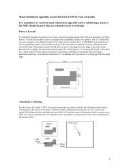
Procedure for gluing silicon wafers together<br />
Silicon pieces (< 4 inch) must be glued to a 4 inch silicon carrier wafer in order for the<br />
loading mechanism to work. Additionally, if a wafer is to be etched all the way through,<br />
the wafer must either have an oxide on the backside or be glued to a 2 nd silicon 4 inch<br />
wafer. This is because backside Helium cooling is used on the wafer chuck and once the<br />
etch breaks through, the helium leaks into the chamber, raises the pressure and shuts<br />
down the machine.<br />
Only silicon carrier wafers are used and must be very clean like the sample to be<br />
etched. The wafer may be either bare silicon or thermally oxidized silicon. A bare silicon<br />
carrier wafer will slow down the etch-rate due to loading effects. For shallow etches, where<br />
very fine control is required, this may be desirable. An oxidized carrier wafer will not load<br />
down the etch and will result in faster etch rates but less control. This may be desirable<br />
for deep etches where speed is required.<br />
The following procedure must be used for etching either wafer pieces or all the way<br />
through the wafer. It is extremely important that no air bubbles be trapped in the<br />
PR as this will cause the piece to flip over during pumpdown or etch. You should<br />
firmly rub the piece onto the 4 inch wafer to remove air and/or use the vacuum bake oven.<br />
Additionally grooves on the underside of your piece will aid in allowing air to escape.<br />
PIECES:<br />
1 Use a Q-tip swab to dab a small drop of AZ5214 resist (or equivalent) on the<br />
backside of your piece.<br />
2 Then carefully center the backside of your piece onto the front-side of the carrier<br />
wafer and press down firmly. Do NOT use too much resist as this will be squeezed<br />
out from the back when you press down and can cause problems.<br />
3 Bake your sample on a hot plate at 120°C for at least 3 minutes. This hardens the<br />
resist. Do not allow the backside of the carrier wafer to become contaminated (eg<br />
from the hot plate).<br />
4 Let your sample cool and bring it to the DRIE machine and follow the loading<br />
procedures as outlined in the SLR 770 <strong>ICP</strong> spec.<br />
WHOLE WAFERS<br />
1 Use a Q-Tip swab as above but put 2 or 3 small drops on the backside of your 4 inch<br />
wafer near the center spaced about 1/2 inch apart.<br />
2 Carefully center the backside of your wafer over the carrier wafer and press down<br />
firmly. Make sure the flats for both wafers line up before pressing the substrates<br />
together.<br />
3 Bake your sample on a hot plate at 120°C for at least 3 minutes. This hardens the<br />
resist. Do not allow the backside of the carrier wafer to become contaminated (eg<br />
from the hot plate).<br />
4 Let your sample cool and bring it to the DRIE machine and follow the loading<br />
procedures as outlined in the SLR 770 <strong>ICP</strong> spec.