
Create successful ePaper yourself
Turn your PDF publications into a flip-book with our unique Google optimized e-Paper software.
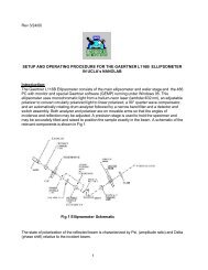
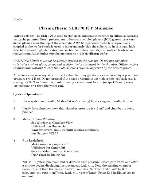
3/11/05<br />
<strong>PlasmaTherm</strong> <strong>SLR770</strong> <strong>ICP</strong> <strong>Minispec</strong><br />
Introduction: The SLR 770 is used to etch deep anisotropic trenches in silicon substrates<br />
using the patented Bosch process. An inductively coupled plasma (<strong>ICP</strong>) generates a very<br />
dense plasma near the top of the electrode. A 2 nd RIE generator which is capacitively<br />
coupled to the wafer chuck is used to independently bias the substrate. In this way, high<br />
selectivities and high etch rates can be obtained. The chemistry can only etch silicon or<br />
(polysilicon). All samples must be mounted to a 4 inch silicon wafer.<br />
CAUTION: Metals must not be directly exposed in the plasma. Do not put any other<br />
substrates such as glass, compound semiconductors or metal in the chamber. Silicon wafers<br />
thinner than 400 and thicker than 600 microns must be approved by the area engineer.<br />
After long runs or many short runs the chamber may get dirty as evidenced by a poor base<br />
pressure (>3.2 E-6). Do not proceed if the base pressure is too high or the leakback rate is<br />
too high (>.3mT in 3 minutes). Additionally a clean must be run (recipe O2clean) every<br />
100 microns or 1 thru the wafer run.<br />
System Operation:<br />
1 Place system in Standby Mode (if it isn’t already) by clicking on Standby button.<br />
2 Verify from chamber view that chamber pressure is
<strong>PlasmaTherm</strong> <strong>SLR770</strong> <strong>ICP</strong> <strong>Minispec</strong><br />
NOTE 2: Make any thickness or depth measurements before processing if you need<br />
to measure selectivity eg photoresist or oxide thickness on Nanospec etc.<br />
NOTE 3: If throttle valve is closed on chamber view, make sure system is in<br />
Standby and go to ServiceMaintenancePumpSystem<br />
5 To load wafer (make sure wafer is clean and resist is hardbaked to at least 120°C)<br />
UtilitiesLoadlockVent<br />
Go to Overview view<br />
On schematic, “At atmosphere” is displayed and lid pops after a few minutes.<br />
Open lid and place wafer flat against chuck etchside up. (Substrates less than<br />
4 inches in diameter must be “glued” to a standard 4 inch wafer. See<br />
Additional Information section of this document for more detail).<br />
6 Pump down load lock:<br />
Close lid and apply gentle pressure<br />
UtilitiesLoadlockPump<br />
In loadlock view after a few minutes red changes to white and pressure reads<br />
~.5 mTorr<br />
7 Transfer wafer to process chamber:<br />
Go to chamber overview window<br />
ServiceMaintenanceWafer Handling<br />
Press Load button on the bottom left of the screen<br />
An animation shows wafer being transferred.<br />
When wafer is transferred and loadlock valve is closed, press Exit button.<br />
8 Verify chamber is being pumped by going to chamber view.<br />
9 Run Leakcheck again:<br />
Make sure ion gauge is off<br />
UtilitiesIon Gauge Off<br />
ServiceMaintenanceLeak Test<br />
Push Start in Dialog box<br />
Note: System pumps chamber down to base pressure, closes gate valve and after a<br />
minute begins displaying instantaneous leak rate. Note the starting chamber<br />
pressure, and then the pressure after 3 minutes. Subtract and divide by 3 to<br />
calculate leak rate in mT/min. Want
<strong>PlasmaTherm</strong> <strong>SLR770</strong> <strong>ICP</strong> <strong>Minispec</strong><br />
Use most recent data from logsheet or test run for etch rate data. Divide<br />
desired thickness (µm) by etch rate to get time (min). CAUTION: Etch rate is<br />
a function of chamber history, % exposed silicon and many other factors. When<br />
in doubt make a test run with an identical sample.<br />
ProcessChamberOpen<br />
Select recipe from list and OK<br />
Double click on Loop Step to set the time in Step 7.<br />
Use the up down arrows to adjust the number of loops (the dep/etch time is<br />
shown to the right of the loop counter).<br />
Make sure Step 4 is highlighted in the Dialog Box as this determines the loop<br />
starting point.<br />
Click OK<br />
Save Recipe?Yes<br />
Exit<br />
11 Load and run recipe<br />
ProcessChamberLoad<br />
Select recipe to load, Press “OK”<br />
Verify desired recipe is shown in “Process” box at lower right screen<br />
Put machine into Ready mode, press Ready button<br />
Press Run to begin processing<br />
12 Verify in Dialog box that correct recipe is running and parameters are correct. It is<br />
a good idea, if at all possible, to stay and make sure the process runs correctly.<br />
13 After etch is completed, click OK in Dialog box, if the Dialog box is present<br />
(Depends on how program was run.)<br />
14 Put machine in Standby mode by pressing Standby button.<br />
15 Transfer wafer to loadlock:<br />
ServiceMaintenanceWafer Handling<br />
Press Unload at bottom of screen<br />
After wafer is in Loadlock press Exit<br />
16 Vent Loadlock as before:<br />
Go to Loadlock View then,<br />
UtilitiesLoadlockVent<br />
17 After lock vents, remove wafer close lid and pump loadlock down again:<br />
UtilitiesLoadlockPump<br />
18 Leave system in Standby mode and record all data in logbook.
Procedure for gluing silicon wafers together<br />
Silicon pieces (< 4 inch) must be glued to a 4 inch silicon carrier wafer in order for the<br />
loading mechanism to work. Additionally, if a wafer is to be etched all the way through,<br />
the wafer must either have an oxide on the backside or be glued to a 2 nd silicon 4 inch<br />
wafer. This is because backside Helium cooling is used on the wafer chuck and once the<br />
etch breaks through, the helium leaks into the chamber, raises the pressure and shuts<br />
down the machine.<br />
Only silicon carrier wafers are used and must be very clean like the sample to be<br />
etched. The wafer may be either bare silicon or thermally oxidized silicon. A bare silicon<br />
carrier wafer will slow down the etch-rate due to loading effects. For shallow etches, where<br />
very fine control is required, this may be desirable. An oxidized carrier wafer will not load<br />
down the etch and will result in faster etch rates but less control. This may be desirable<br />
for deep etches where speed is required.<br />
The following procedure must be used for etching either wafer pieces or all the way<br />
through the wafer. It is extremely important that no air bubbles be trapped in the<br />
PR as this will cause the piece to flip over during pumpdown or etch. You should<br />
firmly rub the piece onto the 4 inch wafer to remove air and/or use the vacuum bake oven.<br />
Additionally grooves on the underside of your piece will aid in allowing air to escape.<br />
PIECES:<br />
1 Use a Q-tip swab to dab a small drop of AZ5214 resist (or equivalent) on the<br />
backside of your piece.<br />
2 Then carefully center the backside of your piece onto the front-side of the carrier<br />
wafer and press down firmly. Do NOT use too much resist as this will be squeezed<br />
out from the back when you press down and can cause problems.<br />
3 Bake your sample on a hot plate at 120°C for at least 3 minutes. This hardens the<br />
resist. Do not allow the backside of the carrier wafer to become contaminated (eg<br />
from the hot plate).<br />
4 Let your sample cool and bring it to the DRIE machine and follow the loading<br />
procedures as outlined in the SLR 770 <strong>ICP</strong> spec.<br />
WHOLE WAFERS<br />
1 Use a Q-Tip swab as above but put 2 or 3 small drops on the backside of your 4 inch<br />
wafer near the center spaced about 1/2 inch apart.<br />
2 Carefully center the backside of your wafer over the carrier wafer and press down<br />
firmly. Make sure the flats for both wafers line up before pressing the substrates<br />
together.<br />
3 Bake your sample on a hot plate at 120°C for at least 3 minutes. This hardens the<br />
resist. Do not allow the backside of the carrier wafer to become contaminated (eg<br />
from the hot plate).<br />
4 Let your sample cool and bring it to the DRIE machine and follow the loading<br />
procedures as outlined in the SLR 770 <strong>ICP</strong> spec.
Additional Information on DRIE<br />
1 For resist thicknesses < 2-3 µm, edge bead removal is probably not necessary if the<br />
resist is baked. Thicker films > 8µm, can outgas and cause clamping problems.<br />
Removal of the edge bead is advised in these cases.<br />
2 Resist profile will affect the etch and sidewall profile. When baking resist, avoid too<br />
high a temperature such that the resist flows (unless you are trying to get a taper).<br />
3 Small silicon pieces can be “glued” to a 4 inch silicon wafer using a dab of PR. If an<br />
oxidized wafer is used, the etch rate will be very fast which may lead to control<br />
problems. A bare silicon wafer will slow the etch down for better control. In any<br />
event, you must use a 4 inch wafer as a carrier.<br />
4 Silicon etch rate is a strong function of exposed silicon (usually expressed as % open<br />
Si). Etching slows down dramatically as the amount of exposed area goes up, so<br />
keeping track of exposed area is important.<br />
5 Some standard Bosch specs for 10-15% exposed area are:<br />
* 1-3 µm/ minute silicon etch rate<br />
* Large open areas etch faster than smaller<br />
* Uniformity of etch and other parameters within 5% across 4 inch wafer<br />
* 75-80:1 selectivity to PR for 12% open Si and 2-100 µm lines<br />
* ~150:1 selectivity to thermal oxide (12% open Si area); PECVD oxide not as good.<br />
* Sidewall angle depends on aspect ratio (Depth to width of trench) and is 88-92<br />
Deg. If process is tuned for 90 Deg at 20 µm, then larger openings will be reentrant<br />
(neg Slope). Conversely if the process is tuned for 90 Deg at larger<br />
openings, a positive taper will result at smaller openings.<br />
6 Run to run uniformity should be about 2 %.<br />
7 For open areas >20%, a bulls-eye pattern can be seen with outer edges etching<br />
faster than the center due to mass loading/gas depletion effects.<br />
8 A seasoning run should be made after opening the process chamber or doing any<br />
substantial maintenance. This involves running the standard Bosch process on a<br />
dummy silicon or oxide wafer (to protect cathode). Depending on total etch time,<br />
some haze may be seen at wafer edges and is considered normal.<br />
9 A cleaning run is not normally needed unless the process chamber is opened and<br />
the fixturing is changed. If so the recipe is:<br />
* 80 sccm O2 + 20 sccm Ar @12 mT
* For 5 “ 500W <strong>ICP</strong> + 100W RIE<br />
* For 15’ 750W <strong>ICP</strong> + 10W RIE<br />
* Make sure a blank wafer is on cathode to protect it<br />
10 Materials that should not be used in the deep RIE include any metal masks. Metals<br />
tend to sputter and contaminate the chamber and clamp and shift the process.<br />
Polyimide and TEOS are OK but a de-scum is highly recommended for polyimide.<br />
11 A mixture of SF6 and O2 can be used to de-scum in the DRIE. Experiments need to<br />
be run to characterize this process.<br />
12 For thru wafer etching, a thick enough mask must be used (oxide has better<br />
selectivity and therefore doesn’t require as thick a layer. When the etch completes,<br />
the backside helium cooling fails and requires stopping the process. At this point<br />
short runs of no longer than 5 minutes with He cooling off followed by a 5 minute<br />
cool-down may be run to finish the etch.<br />
A better alternative is to have an oxide on the other side of the wafer which may be<br />
used as an etch-stop and so maintains a seal to keep the He cooling on. The<br />
backside oxide must be thick enough to accommodate whatever overetch after<br />
breakthru is required.<br />
A third alternative is to glue the wafer to be etched to a 2 nd carrier wafer so that He<br />
cooling is maintained.<br />
13 A dielectric substrate (eg quartz) instead of a semiconductor may only be used with<br />
the area engineer’s approval and most likely will require special setup. For<br />
dielectrics, a parasitic capacitance is introduced which interferes with the bias and<br />
therefore the etching of the substrate. Too low a bias indicates the capacitance<br />
problem.<br />
14 <strong>PlasmaTherm</strong> has done oxide etching in the DRIE without any obvious problems,<br />
but they do not guarantee anything and they are concerned that it may affect the<br />
Bosch process.<br />
15 After running processes in the <strong>ICP</strong> pressure will degrade with time. Background<br />
pressure in the 10-5 range is normal. Etching is a dirty process especially with the<br />
deposition of polymers which is an essential part of the Bosch process.<br />
16 To see if the chamber is clean enough (or vacuum low enough), run bare Si wafer for<br />
20 ‘ using standard Bosch process. If wafer looks clear to the high (eg no haze), then<br />
system is clean enough.<br />
17 During SEM examination, some charging due to existence of polymer may be seen.<br />
Recommend sputter coating rather than ashing to obtain better image.
18 During the deposition of the standard Bosch process, approximately 1000 Å of<br />
polymer is deposited.<br />
19 <strong>PlasmaTherm</strong> has measured the temperature of the wafer during a standard 20’<br />
Bosch run as between 40-50 °C. The clamp however can go as high as 80°C.
MISCELLANEOUS PROBLEMS<br />
SYSTEM LOCKUP<br />
Occasionally the system may lock up and not respond to any commands. Try exiting the<br />
Program Sysmon if possible or if that doesn’t work try exiting windows and restarting<br />
(type win after getting the DOS prompt). If this fails, open the lower panel and press the<br />
red reset button on the computer at the bottom. This should reboot all the software and a<br />
dialog box requesting user and password will come up. Enter 3333 in both boxes. If a<br />
wafer is in the process chamber it should still know this. Verify if the turbopump is on by<br />
checking the column of green lights on the back of the machine. If off, turn on the<br />
turbopump from the menu and wait 10-15 minutes for vacuum to recover . If that doesn’t<br />
work, get help.<br />
IDENTIFYING & ACKNOWLEDGING ALARMS<br />
If something went wrong and you are not sure what happened (check info box at the<br />
bottom of screen first) go to:<br />
Display!Alarm History<br />
Date and time appear next to each alarm and can help you identify what went wrong.<br />
Press ALARM SILENCE at the bottom right of screen to silence an alarm or at the end of<br />
a run. If there is a problem, the HOLD button illuminates when the alarm is silenced.<br />
Push the HOLD button to put the system back in Standby or Ready. If the alarm condition<br />
is still present, however, the alarm will continue to go off. In this case the problem must<br />
be fixed first.<br />
UNLOADING PROBLEMS<br />
Wafer transfer problems generally occur because of either poor procedure of attaching a<br />
wafer to a carrier or thick PR at the wafer edge which gets sticky with heat causing the<br />
wafer to stick to the clamp and break in the process chamber. For thicker resist, use edge<br />
bead removal or keep your etches short. For gluing wafers use very small dabs of<br />
photoresist or approved material and bake thoroughly. If a wafer breaks or gets stuck in<br />
process chamber, you must get help. Do not attempt to fix the problem yourself.<br />
CHAMBER CLEANING<br />
As mentioned previously, an oxygen plasma clean (recipe O2Clean) should be run every 8<br />
hours or so of etching for 15 minutes. Load the dummy clean wafer kept at the machine<br />
and load the recipe following standard procedures. Make the entry in the log book that the<br />
O2Clean was run. There is no charge for this.<br />
MORPHING<br />
It is common for the etch rate to slow down as the trench gets very deep (ie the aspect<br />
ratio gets high). Morphing is a software feature which allows a variable to be<br />
automatically incremented as a dep/etch loop is completed. Usually the RIE power is<br />
incremented as the trench gets deeper. The rate of change ie sublinear, logarithmic etc can<br />
be programmed as well. However you must work with a superuser or lab management to<br />
use this feature.
ADDITIONAL RECIPES<br />
An approved recipe list is kept at the machine. You must get approval and help in writing<br />
your own recipe since small changes in a parameter can have a large detrimental effect on<br />
the process and machine. Once the recipe is approved it will be added to the recipe list.<br />
Anyone may run any of the posted recipes but may change only the etch time, nothing<br />
else.<br />
SYSTEM ABORT<br />
The abort button at the bottom of the screen aborts the entire recipe but may cause a<br />
system crash. If possible try using End Step several times first.<br />
EMERGENCY SHUT OFF<br />
The big red button at the front side of the machine will kill all the power and is to be used<br />
only in extreme emergency ie smoke or burning smell coming from the machine, etc. Do<br />
NOT attempt to turn on the machine if it is shut down in this manner.<br />
GAS SUSPECTED IN CHAMBER<br />
This alarm may occur from a system abort, a logic error or a real problem. If the turbopump<br />
is still on (green) and the throttle valve is closed (as seen in Chamber View) try<br />
pumping the system in the Standby mode by selecting:<br />
Service!Maintenance!Pump!System