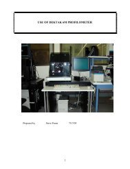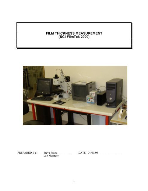
FILM THICKNESS MEASUREMENT (SCI FilmTek 2000)
FILM THICKNESS MEASUREMENT (SCI FilmTek 2000)
FILM THICKNESS MEASUREMENT (SCI FilmTek 2000)

Create successful ePaper yourself
Turn your PDF publications into a flip-book with our unique Google optimized e-Paper software.
PREPARED BY:<br />
<strong>FILM</strong> <strong>THICKNESS</strong> <strong>MEASUREMENT</strong><br />
(<strong>SCI</strong> <strong>FilmTek</strong> <strong>2000</strong>)<br />
Steve Franz DATE<br />
Lab Manager<br />
1<br />
04/01/03
1.0 SCOPE<br />
<strong>FILM</strong>TEK <strong>2000</strong> <strong>THICKNESS</strong> <strong>MEASUREMENT</strong><br />
This document establishes the procedures for film thickness measurements<br />
using the Filmtek <strong>2000</strong> in the Nanoelectronics laboratory.<br />
2.0 APPLICABLE DOCUMENTS<br />
Filmtek logbook and maintenance log<br />
<strong>FilmTek</strong> Operations Manual<br />
3.0 MATERIALS AND EQUIPMENT<br />
<strong>FilmTek</strong> <strong>2000</strong><br />
<strong>FilmTek</strong> Si reference wafer<br />
Tweezers<br />
4.0 INTRODUCTION<br />
The <strong>FilmTek</strong> <strong>2000</strong> is a spectrophotometer capable of measuring a reflected<br />
beam from the UV (280nm) through the visible and near IR (1700nm). Based<br />
on software integrated into the <strong>FilmTek</strong> computer, film thicknesses and<br />
refractive indexes of multiple layers can be measured. In some cases, extinction<br />
coefficients and even bandgap or doping can be measured. Care must be<br />
taken, however, since for some cases eg numerous multiple thin layers, a<br />
unique solution may not exist and another measurement technique must be<br />
used. Examples of films that can be measured include: very thin oxides or<br />
nitrides, polymer films, silicon on oxide (SOI) film stacks, III-V heterostructures,<br />
porous Si films etc..<br />
4.1 Principal of Operation<br />
A light source of the desired wavelength range is used to shine light at normal<br />
incidence through a focussing system to form a spot on the sample surface. The<br />
reflected beam is sent through the appropriate optical path to the detector. A<br />
beam splitter, usable only in the visible, is used to display the image on a video<br />
screen. The splitter must be removed from the optical path for UV<br />
measurements. There are 3 detectors selectable by software; one for each<br />
wavelength range. There are also 3 light sources used for our system: a<br />
deuterium lamp for UV wavelengths, a halogen lamp for visible and IR<br />
wavelengths and a microscope lamp for visible and IR wavelengths. The<br />
halogen lamp is usually not needed and should be left off.<br />
Absolute reflection data is obtained by comparing sample reflection to the<br />
measured reflection of a user supplied reference substrate. Using a generalized<br />
material models in combination with advanced global optimization algorithms<br />
and power spectral density analysis, <strong>FilmTek</strong> can simultaneously determine:<br />
Multiple layer thickness<br />
Indices of refraction [ n(λ) ]<br />
Extinction (absorption) coefficients [ k(λ) ]<br />
2
The parameters that are solved for, along with the layer structure of the sample<br />
being measured, are stored in recipes. The <strong>FilmTek</strong> computer contains many<br />
commonly used recipes and the user can modify these recipes and create new<br />
recipes. The measurement sequence is initiated by clicking a single button in<br />
the <strong>FilmTek</strong> Main Window. The spectrophotometer scans the sample over a<br />
predefined range of wavelengths. The software generates a corrected spectrum<br />
based on a previously stored reference scan, and then performs a regression<br />
on the unknown parameters to fit the simulated reflection and power spectral<br />
density to the their observed values. The resulting thin film parameters along<br />
with the measured and modeled spectra are then displayed for the user to<br />
examine.<br />
<strong>FilmTek</strong> can precisely measure virtually all translucent films ranging in<br />
thickness from less than 100 angstroms to approximately 50 microns. Typical<br />
applications include:<br />
Semiconductor and dielectric materials<br />
Computer disks<br />
Optical antireflection coatings<br />
Coated glass<br />
Electro-optical materials<br />
Laser mirrors<br />
Multilayer optical coatings<br />
Thin Metals<br />
5.0 SYSTEM SET UP AND OPERATION<br />
5.1.1 Turning on the system<br />
The computer and microscope lamp should be left on but the Deuterium lamp<br />
and Halogen lamp should be left off when not in use. You only need to use the<br />
Deuterium lamp if you need to use UV wavelengths. You only need to use the<br />
Halogen lamp if you are using visible or IR AND you are not getting enough<br />
signal from the microscope lamp. To turn on the various lamps (see Fig 1):<br />
Fig 1. Filmtek Lamp Power Supply<br />
3
5.1.2 Deuterium Lamp (UV)<br />
To turn on the deuterium lamp (UV only):<br />
NOTE: The LED below the lamp switch is green if the power is on.<br />
1 Verify that the main power is on (green LED labeled power).<br />
2 Turn off the halogen lamp if it is on (red button) and<br />
3 Press the blue button and wait 10 seconds. The green LED below<br />
the blue (deuterium ) lamp switch should come on; if not press the blue<br />
switch again. If you need to turn back on the halogen lamp, simply<br />
press the red button.<br />
4 If the Deuterium LED turns on red, press the blue button again.<br />
NOTE: Both lamps should be warmed up for 10 minutes before using.<br />
To turn off the deuterium lamp :<br />
Simply press the blue button and the green LED should go out indicating<br />
the lamp is off. The lamp should be left off when not in use to prolong its<br />
life.<br />
5.1.3 Halogen Lamp (Visible & IR)<br />
To turn on the halogen lamp simply press the red button and the green<br />
LED should come on. To turn it off, press the red button again. Normally<br />
the halogen lamp may be left off since the microscope lamp contains<br />
enough energy for the visible and IR spectrum.<br />
5.2 Microscope Set Up<br />
Fig 2. Filmtek <strong>2000</strong> Microscope<br />
4
CAUTION: Adjust ONLY those knobs discussed below. Do NOT tamper with any<br />
other knobs or filters.<br />
1 Make sure the appropriate light source is on (section 5.1.1 and 5.1.2)<br />
and that the microscope lamp is on as well (Fig 2). The field diaphragm<br />
and aperture should be closed down all the way (levers down).<br />
2 To image a sample, place a sample on the stage and select one of the<br />
silver objectives by rotating it into position. Do NOT use the black<br />
objective for viewing an image; this is only to be used for taking<br />
measurements in the UV range.<br />
3 Make sure the UV-Vis shutter is in the “in” position. It is also labeled<br />
BF/DF on the microscope body.<br />
4 All images are viewed on the TV monitor which is left on. Adjust the focus<br />
knob located at the base of the microscope. If your sample has no<br />
features, focus to get a sharp image of the field diaphragm edge.<br />
5 The lamp on/off switch is located at the rear base of the microscope and<br />
should be left on. Lamp intensity may be adjusted by the knob at the<br />
bottom left of the scope (Fig 2). This should be adjusted to get the<br />
appropriate signal level as discussed in section 5.1.5.<br />
5.3 Computer Set Up<br />
The computer is usually left on but may need to be woken up from the sleep<br />
mode by pressing a key. It may also be rebooted following standard Windows<br />
procedures. No password is required. The system runs on Windows XP and has<br />
both a CDROM drive (top bay) and CD-Write drive (bottom bay) as well as a<br />
standard floppy drive. Data may be exported as ascii text files or graphic<br />
metafiles to CD or floppy depending on file size.<br />
5.4 System Operation<br />
1 From the Windows desktop, double click on the Filmtek icon to start the<br />
program. The program opens with the main window as shown in Fig 3.<br />
Fig 3. Startup screen for Filmtek Program<br />
5
2 Unless you will use a stored recipe and don’t need to make any changes,<br />
you will need to log in as a power user. To do so, click on “Security” on<br />
the pull down menu and select “Log-in”. Type in User Name: <strong>SCI</strong> and<br />
the password located on the cover of the <strong>FilmTek</strong> manual. Also select<br />
“Power user” (Fig 4).<br />
Fig 4. Log in screen<br />
3 Click the recipe pull down menu at the bottom right of the screen and<br />
scroll to the desired program.<br />
Programs will have a descriptive name for the film and substrate to be<br />
measured as well as a suffix UV, vis (visible) or ir for the appropriate<br />
wavelength range. The microscope must be set up correctly for the<br />
wavelength range being measured as well. If the desired recipe does not<br />
exist contact lab staff or the appropriate engineer to assist in designing a<br />
program. In some cases samples may need to be sent to <strong>SCI</strong> for initial<br />
characterization. In all cases a known standard must be used to<br />
insure that meaningful measurements are being taken.<br />
4 Make sure the appropriate lamp is on (section 5.1.1 and 5.1.2). The<br />
microscope lamp should always be on for sample viewing and as a<br />
visible/ir source.<br />
5 Choose the appropriate objective lens (silver for visible/IR, black for UV)<br />
and position the light beam over the center hole in the wafer stage with<br />
NO SAMPLE.<br />
6 If you are using UV also make sure the UV-vis shutter is “out”. For visible<br />
and IR it should be “in”.<br />
7 For IR, choose “Calibration”->”NIR Settings” and click the enable box at<br />
the bottom left. The integration time may be changed here as well (see<br />
step 11).<br />
8 Press the “Background” button in the toolbar (2 nd button from the left). A<br />
graph with a red line at 0 should be displayed.<br />
This step is to zero the machine taking into account ambient and stray light. It<br />
should be done hourly or whenever a recipe is changed.<br />
9 Place the <strong>SCI</strong> silicon reference wafer shiny side up on the microscope<br />
stage and position the wafer under one of the visible (silver) objectives.<br />
Focus on a clean spot on the wafer so that the field diaphragm presents a<br />
nice sharp edge. UV-vis shutter should be in.<br />
10 For UV: Select the black objective lens, pull out the UV-vis shutter and<br />
press “Reference” on the toolbar (leftmost icon-Fig 3). For visible/IR:<br />
Simply press “Reference” on the toolbar (leftmost icon-Fig 3). Press<br />
6
“Rescale” to update the graph.<br />
This step calibrates the reflectance axis to a known standard (eg silicon)<br />
so that it correctly reads in % instead of counts. . It should be done hourly<br />
or whenever a recipe is changed. Other standards can be used eg glass<br />
or other semiconductors but the program must be set up explicitly for this<br />
in advance. The <strong>SCI</strong> manual discusses this in more detail.<br />
11 A spectrum for the reference reflectance will be displayed as shown in<br />
Fig 5 for visible and Fig 6 for UV. The counts should be between 1000-<br />
<strong>2000</strong> (for a silicon reference). To adjust signal strength for visible/IR,<br />
)<br />
s<br />
t<br />
n<br />
u<br />
o<br />
c<br />
(<br />
l<br />
a<br />
n<br />
g<br />
i<br />
S<br />
50 00<br />
45 00<br />
40 00<br />
35 00<br />
30 00<br />
25 00<br />
20 00<br />
15 00<br />
10 00<br />
50 0<br />
0<br />
20 0 30 0 400 500 600 700 80 0 90 0<br />
Wavelength (nm)<br />
Fig 5. Visible spectra for silicon reference wafer properly scaled.<br />
)<br />
s<br />
t<br />
n<br />
u<br />
o<br />
c<br />
(<br />
l<br />
a<br />
n<br />
g<br />
i<br />
S<br />
5000<br />
4500<br />
4000<br />
3500<br />
3000<br />
2500<br />
<strong>2000</strong><br />
1500<br />
1000<br />
500<br />
0<br />
200 300 40 0 500 60 0 700 80 0 90 0<br />
Wavelength (nm)<br />
Fig 6. UV spectra for silicon reference wafer properly scaled.<br />
7
the lamp intensity may be adjusted or the integration time may be<br />
adjusted (for UV, only the integration time may be adjusted).<br />
Select “Calibration” in the pull down menu and then choose “Data<br />
Collection”. Select “Integration time”. Decrease the time to reduce the<br />
count or increase the time to increase the count. Excessively noisy<br />
signals may be improved by increasing “Samples to Average” or<br />
increasing “Data Smoothing”. Verify also that the appropriate detector is<br />
selected: UV= detector 1 and Visible = detector 2.<br />
The real time signal from the detector may be checked any time by<br />
clicking on the “Signal” button (2 nd from right in Fig 3). It may be<br />
necessary to refresh the display by pressing “Data” or “Graph” and then<br />
pressing “Signal” a 2 nd time. To check that the displayed signal is real<br />
time, rotate the objective to block the light and after a few seconds delay,<br />
the display should go to 0; if not, you must refresh the display.<br />
12 Remove the silicon reference wafer and put it in the covered wafer<br />
holder.<br />
13 Place the sample to be measured on the stage and position the stage<br />
under the appropriate objective lens (silver for visible/IR, black for UV).<br />
14 With the UV-vis shutter in, focus so that the field diaphragm edge is in<br />
focus.<br />
15 For Visible/IR, press “Measure” button on the toolbar to initiate<br />
measurement. For UV, pull shutter out and make sure black objective is<br />
in place. Press “Measure”.<br />
16 After a few seconds, a blue curve for the measured values is displayed<br />
along with the red simulated curve. If Autosolve is enabled (usually the<br />
case), it is not necessary to press “Solve” again.<br />
17 The fitted parameters appear in 3 columns along the right side of the<br />
display: name of parameter, initial value and final solution. Also the n and<br />
k at a predetermined wavelength for a predetermined layer (usually layer<br />
1 at 632 nm) are shown.<br />
18 The root mean square error RMSE is shown at the bottom and if it is<br />
greater than a preprogrammed limit, an error message will be displayed.<br />
In general, you want the RMSE to be small ( “Save Data” and give it a descriptive<br />
name. Use the default “Data” folder that pops up. Recipes, data and<br />
modeling parameters must be in the proper default folders or the<br />
program won’t be able to access them. Data can be saved as editable,<br />
formatted text by using the report feature (see Filmtek manual).<br />
20 If there is a problem with the data, you can try changing parameters in the<br />
layers/settings dialog box (“Setup”->”Model/Layers Settings”). You can<br />
8
try extending the range of the film thicknesses, adding a layer (eg native<br />
oxide or interfacial layer) or changing the parameter to be fitted. Press<br />
“Solve” after making the changes and compare the curves and RMSE<br />
again.<br />
Care should be taken in adjusting materials or modeling parameters. It is<br />
possible to get a good fit but the wrong result since there are so many<br />
parameters which can be used to fit the curve. See the appropriate lab staff or<br />
superuser if you are having serious problems.<br />
21 When finished using the machine, remove your sample, close the<br />
program and turn off the deuterium or halogen lamp if no one else is<br />
planning on using the machine.<br />
22 Fill in the log book and enter any problems in the comments section.<br />
6.0 RECIPES<br />
6.1 General<br />
In general it is recommended that you get help for generating new recipes but in<br />
some cases, for example for a thicker or thinner film, an existing recipe may be<br />
modified fairly simply to make the measurement. In that case it should be saved<br />
under a new descriptive name with the appropriate tag: vis for visible, uv or ir<br />
(“File”->”Save Recipe as”. A more complete discussion of recipes and<br />
parameters is given in the Filmtek operation manual but some suggested<br />
guidelines are:<br />
1 Try to limit the Film Thickness to the smallest range possible. Generally,<br />
from the reflection spectrum one can deduce what limits should be used.<br />
• If there are a number of maxima and minima in the spectrum, the film<br />
thickness is greater than 1000 Angstroms. The more swings in the<br />
spectrum, the thicker the film is. If the spectrum does exhibit maxima and<br />
minima, be sure to use Thick Film Optimization techniques.<br />
• If the spectrum is monotonic either the film is thin (< 100 nm) or highly<br />
absorbing. If the film is highly absorbing, film thickness may not be<br />
determinable.<br />
2 When fitting on index and the material is known, if available, start with a<br />
model which describes the material. For example, if it is known that the<br />
material is Aluminum, start with a Material Model that describes<br />
Aluminum. Also use constrained optimization on the Material<br />
Coefficients. In the appendix of the Filmtek manual, there is a table<br />
showing <strong>SCI</strong> Model Material Coefficients for many common materials.<br />
3 Use as few fitted parameters as possible to solve the problem.<br />
4 If the spectrum does exhibit maxima and minima, be sure to use Thick<br />
Film Optimization techniques.<br />
5 When fitting on index and it is known that the film has no absorption, use<br />
the <strong>SCI</strong> Material Model and set the High Dielectric Constant to 1, the<br />
9
damping coefficient to zero, the Vibrational Frequency to zero, and do not<br />
fit on any of these parameters.<br />
6 When solving for an unknown dielectric material which does exhibit<br />
absorption in part of the spectrum, it sometimes best to solve the problem<br />
in parts. The procedure is as follows:<br />
• Limit the wavelength range to that part of the spectrum where the film is<br />
transparent.<br />
• Use the <strong>SCI</strong> Material Model with a single oscillator. Set the High<br />
Dielectric Constant to 1, the damping coefficient to zero, the Vibrational<br />
Frequency to zero, and do not fit on any of these parameters. Solve for<br />
thickness, Amplitude and Center Energy.<br />
• Include the entire wavelength range.<br />
• Solve again, fitting only on Vibrational Frequency, Damping Coefficient,<br />
and High Dielectric constant.<br />
• Next, fit on all parameters.<br />
• If the fit is not satisfactory, add another oscillator fitting on all<br />
parameters. Starting values for another oscillator are :<br />
Value Max Min<br />
High Dielectric Constant 1 3 1<br />
Damping Coefficient 025 1 0<br />
Amplitude 15 30 0<br />
Center Energy 7 30 2<br />
Vib. Freq. 1 5 0<br />
7 For very thin films, it is usually best to use the UV wavelength range to get a<br />
sufficient number of cycles (interference fringes). Don’t use UV for highly<br />
absorptive thick layers or a thick film stack where the beam cannot penetrate<br />
to the desired interfaces.<br />
8 For some III-V heterostructures or SOI layers, IR may be a good choice. In<br />
this case the light can penetrate to the various interfaces but the substrate’s<br />
backside may play a role in the reflected signal and may need to be<br />
accounted for. The reference for example should have the same type<br />
backside (eg polished vs rough) as the sample. The backside reflections<br />
can be included or excluded in the checkbox in the Layers/Settings dialog<br />
box but is not used in calculating the curve.<br />
6.2 The Model Window/Changing Parameters<br />
In the Model Window, the known and unknown film properties of the sample to<br />
be measured are specified. The properties set in the Model Window include :<br />
Number of layers<br />
Thickness of known layers (if any)<br />
Maximum thickness of each layer<br />
Minimum thickness of each layer<br />
Material model or NK file for each layer<br />
Material model or NK file for the substrate<br />
Enable surface roughness measurement (<strong>FilmTek</strong> <strong>2000</strong> only)<br />
Enable the use of Thick Films Optimization Techniques (Fitting on Power<br />
Spectral Density, Filmtek 1000 and <strong>FilmTek</strong> <strong>2000</strong>)<br />
10
Materials may be defined by equation/dispersion formulas (models) or by an NK<br />
file. The available material models include: Sellmeier, Cauchy, Cauchy<br />
Exponential (which is highly recommended for glasses), Drude, Lorentz<br />
Oscillator, and Drude+Lorentz Oscillator. In addition to the above-mentioned<br />
material models, <strong>FilmTek</strong> provides two new generalized dispersion formulas<br />
(<strong>SCI</strong> and Tauc Lorentz Model) which apply to metals, amorphous and<br />
crystalline semiconductors, and dielectric materials. The <strong>SCI</strong> Model is the<br />
only material model you will ever need to model any material . The<br />
Tauc Lorentz model is very useful when it is desired to solve for the band gap<br />
energy.<br />
If the material type is other than NK, the index of refraction values are calculated<br />
from the coefficients of the model equation. These coefficients may be edited in<br />
the Coefficient Table along with their respective maximum and minimum values.<br />
In <strong>FilmTek</strong> the user may fit on the coefficients of an equation based material<br />
model but not directly on the NK values.<br />
The Model/Layer Setting Window is shown below. Each individual parameter is<br />
described below.<br />
Fig 7. Model Layer/SettingsWindow<br />
Number of Layers: This combo box is used to select the number of layers in<br />
the stack. The first layer is the layer next to the substrate. The film stack can be<br />
composed of up to five layers. Zero is selected to specify that no films are on top<br />
of the substrate (zero layers).<br />
Include Substrate Backside:<br />
The user can choose to include or exclude reflections from the second surface<br />
(backside) of the substrate. To include backside reflections simply click on the<br />
box with the mouse and input the substrate thickness in the first row third<br />
column of the layer configuration table (substrate thickness is always specified<br />
in mm).<br />
Note: Since phase information is physically not meaningful for incoherent<br />
layers, the calculation of ellipsometric parameters are completely unaffected by<br />
this check box. <strong>FilmTek</strong> will always ignore the backside reflection in calculating<br />
ellipsometric data. When collecting ellipsometric data, the backside reflection<br />
should be minimized.<br />
Note: One can not fit on the thickness of the substrate. To handle this problem<br />
when the substrate thickness is unknown, make the substrate material VOID or<br />
11
air and set the material of the first layer to the substrate material. Also set the<br />
thickness units of layer 1 to mm, which makes layer 1 a massive or incoherent<br />
layer.<br />
6.3 Layer Configuration<br />
This table is a spreadsheet with eight columns and up to six rows. Each row<br />
represents a different layer in the film stack. The layer number is displayed in<br />
the column zero. Columns one to eight are:<br />
Fit on Thick. : The first column contains a check box labeled ‘Fit’. Checking<br />
this box will cause the layer thickness to be solved for when the measure or<br />
solve button is pressed in the main window.<br />
Thick. : The second column displays the starting layer thickness.<br />
Thick Max. : The third column displays the maximum layer thickness.<br />
Thick Min.: The fourth column displays the minimum layer thickness.<br />
Thick Units: The fifth column is used to display the thickness units of the<br />
associated layer. The user should only select “mm” for layers that are<br />
massive (very thick layers that should be treated as incoherent layers such<br />
as glass substrates).<br />
Material File: The sixth column is used to display the material file name of<br />
the associated layer. To load a previously saved NK file or one of the files<br />
supplied with <strong>FilmTek</strong> click on the combo-box and select one of the listed<br />
material files. Please note that if the Material Model is not NK, then the<br />
Material Model and not the displayed NK file give the nk values. To make<br />
the Material File active, check to see that the Material Model is NK.<br />
Fit on NK: The seventh column contains a check box labeled ‘Fit’. Checking<br />
this box will cause the layer material model coefficients to be solved for<br />
when the measure or solve button is clicked in the main window. Note that<br />
in <strong>FilmTek</strong> the user fits on the coefficients of the equation based material<br />
models rather than directly on the NK values. The Fit on NK button is<br />
disabled whenever the selected Material Model is NK. A utility to convert<br />
NK files to an equation based material model can be accessed from the<br />
main window (Find Coefficients under the Utilities pull down menu).<br />
Material Model: The last column is used to display the material model for<br />
the associated layer.<br />
6.4 Coefficient Table<br />
In the Coefficient Table the user may edit the coefficients of equation-based<br />
materials along with their respective maximum and minimum values . The<br />
number of coefficients necessary to fully describe the material depends on the<br />
particular material model. The Cauchy material model has six coefficients : An,<br />
Bn, Cn, Ak, Bk, Ck. The Sellmeier, on the other hand, has only three<br />
coefficients. In addition to specifying the coefficients along their maximum and<br />
minimum values, in the Coefficient Table the user also specifies which<br />
coefficients will be allowed to vary.<br />
12
The fitted coefficients are defined by checking the small check box in the<br />
second column next to the parameter value to be fitted. It is important to note<br />
that the checked coefficient is not fitted on unless the Fit on NK button located<br />
in the Layer Configuration Table is also checked.<br />
7.0 Sample Problems<br />
7.1 Determining The Thickness of Thick Films (Polyimide on SiO2 on<br />
Silicon:<br />
Problem: To determine the thickness of polyimide on silicon oxide on silicon.<br />
Spectroscopic reflection data at normal incidence (angle of incidence = 0°) is<br />
supplied for this problem on the <strong>SCI</strong> CD ’22 um Polymide on sio2 (2um) on<br />
Si.tar”.<br />
Fig 8. Layer data for polyimide on SiO2 on silicon<br />
Select thick film optimization option (5 th button from left labeled FFT). Click on<br />
the “OK” button after filling in the data to return to the main window. Load the<br />
data file (Data->Open “22 ¨µm Polyimide on sio2 on si.tar”) and click “Solve”.<br />
The solved data graph is displayed as shown in Fig 9.<br />
Fig 9. Solution to polyimide/SiO2/Si<br />
13
To verify number of films, select PSD/FFT button to display the power spectra as<br />
shown in Fig 10.<br />
Fig 10. Power Spectral Density for polyimide problem<br />
The 2 peaks correspond to the SiO2 and Polyimide films.<br />
7.2 Determining the Thickness and Index of SiO2 on Silicon<br />
Problem: To determine the thickness and real index of refraction (n) of silicon<br />
oxide on silicon. Spectroscopic reflection data at normal incidence (angle of<br />
incidence = 0°) is supplied for this problem in “\data\SiO2.tar”. A 13nm SiO2 film<br />
was grown on a silicon substrate. For this example we will load a previously<br />
defined recipe.<br />
Load the SiO2 Recipe by clicking on the combo box labeled Recipe in the lower<br />
right corner of the main window. The Fitted Parameters table is automatically<br />
updated to reflect the unknown variables in the SiO2 recipe. The main window<br />
will appear as shown below.<br />
Fig 11 Main window for SiO2/Si problem<br />
To view or edit the Model click on the Model command button in the tool bar or<br />
select Model/Layer Settings from the Setup pull down menu in the Main<br />
Window. This will bring up the Model/Layer window shown in Fig 12. The first<br />
row in the layer configuration table shows the substrate material (Si) name and<br />
the material model (NK file). The settings for the first layer (SiO2) are shown in<br />
14
the second row, Labeled “Layer #1”. The ‘Fit’ check-box of Row 2 is checked to<br />
allow the thickness of Layer 1 to vary during the optimization. The initial<br />
thickness of the SiO2 is 50nm with a minimum and maximum thickness<br />
constraints of 0 and 600nm.To view the model coefficients of SiO2 click on any<br />
cell in the second row Labeled “Layer #1”. The SiO2 coefficient table is now<br />
visible. The material model (dispersion formula) used for SiO2 in this example<br />
is <strong>SCI</strong>. The extinction coefficient (k) for SiO2 is zero (for wavelength range<br />
between 200nm-4000nm). To set k=0, both the Damping Coefficient and<br />
Vibrational Frequency have been set to zero. Since no changes are made click<br />
on the Cancel button to go back to the main window.<br />
Fig 12. Model layer window for SiO2 problem.<br />
To load the Spectroscopic reflection data (SiO2.tar file) select Open from the<br />
Data pull down menu in the Main Window. This will launch a Windows Common<br />
Dialog Box requesting input of the target file name to be loaded. Select SiO2.tar<br />
file name. The reflection data will now be loaded. The measured and simulated<br />
reflection data will automatically be displayed in the data graph in the main<br />
window .<br />
To begin the optimization click on the Solve Command Button located on the<br />
tool bar or select Solve from the Measure pull down menu in the Main Window.<br />
When the optimization is complete, the Fitted Parameters Table will show both<br />
the initial and final values of the unknown thin film parameters. The final SiO2<br />
thickness is 29.96nm.To re-scale the graph, click on the Rescale Command<br />
Button located in the tool bar. The measured and simulated data is shown in Fig<br />
13.<br />
15
Fig 13. Measured and simulated SiO2 reflection data.<br />
To view the SiO2 NK values click on NK Graph Command Button located on the<br />
tool bar or select NK Graph from the View pull down menu in the Main Window.<br />
To view the substrate (Si) NK values click on the combo box labeled Display in<br />
the lower right corner of the main window and select Substrate.<br />
Fig 14. N and K spectra of SiO2 and Si.<br />
7.3 Determining The Thickness of a Multi-layer Structure (Silicon on<br />
Insulator –SOI):<br />
Problem: To determine the thickness of Layer 1 (Buried Oxide SiO2), Layer 2<br />
(Silicon) and Layer 3 (Gate Oxide SiO2). Spectroscopic reflection data at<br />
normal incidence (angle of incidence = 0°) is supplied for this problem in<br />
“\data\SiO2 On SOI.tar”. The expected film thicknesses are Substrate/390nm<br />
SiO2/209nm Si /12nm SiO2.<br />
16
To define/build a new Recipe Load the Default Recipe by clicking on the combo<br />
box labeled Recipe in the lower right corner of the main window. This resets the<br />
recipe to the default recipe and the main window will appear as shown below.<br />
To edit the Model click on the Model command button in the tool bar or select<br />
Model/Layer Settings from the Setup pull down menu in the Main Window. This<br />
produces the Model/Layer dialog box shown below.<br />
Fig 15. Inputting data in the Modeling/Layer Window<br />
To change the number of layers from 1 to 3 layers click on the combo box<br />
labeled Number of Layers and select 3. The Model/Layer dialog box will<br />
automatically update the layer list as shown above. The first row in the layer<br />
configuration table shows the substrate material (Si) name and material model<br />
(NK file). The settings for the layer 1-3 are shown in rows 2-4. First we need to<br />
change the material of layer 1 from Si2N3 to SiO2. Click on row 2 column 6<br />
(labeled "Material File") and select SiO2. A dialoge box will automatically pop<br />
and ask if you would like to load the SiO2 Coefficients form a previously defined<br />
material file. Select OK. Similarly set the Material of layer two and three to Si<br />
and SiO2 respectively.<br />
Fig 16. Model layers window for SOI problem.<br />
In this example we will not fit on the index of SiO2. To simplify the recipe set the<br />
SiO2 material model to NK.<br />
17
Fig 17 Model layers window for SOI problem (cont’d).<br />
Change the starting thickness of layer one to 430 (nm) and the maximum<br />
thickness to 500 (nm). Set the starting thickness of layer two to 290nm, the<br />
maximum thickness to 400 (nm) and the minimum thickness to 100 (nm).<br />
Similarly set the starting thickness of layer three to 20nm, the maximum<br />
thickness to 100 (nm) and the minimum thickness to 0 (nm).<br />
To solve for the thickness of layers 1-3 the ‘Fit’ check-box (column 1) of Row 2-4<br />
should be checked. To save the new recipe click on File: Save As from the pull<br />
down menu and save the file (SiO2 on Si) for future use. Click the OK button to<br />
accept the changes in the Model/Layers Settings.<br />
Fig 18. Saving the recipe<br />
Before proceeding, we will check the Data Collection Parameters. Select Data<br />
Collection Parameters from the Calibration pull down menu in the Main<br />
Window. This will launch a Data Collection Parameters Dialog Box. The “Limit<br />
Number of Wavelength” parameter is set to 100. In order to speed up the<br />
optimization process, this parameter is used to limit the maximum number of<br />
experimental/measured points. The program automatically selects the<br />
appropriate wavelengths, which are uniformly distributed in frequency space.<br />
Since this example has many oscillations in the data, we will increase the<br />
number of wavelengths from 100 to 300. This will increase the resolution of our<br />
data set.<br />
18
Fig 19 Checking Data collection parameters<br />
Now we are ready to load the data. To load the spectroscopic reflection data<br />
(SiO2 on SOI.tar file) select Open from the Data pull down menu in the Main<br />
Window. This will launch a Windows Common Dialog Box requesting input of<br />
the target file name to be loaded. Select SiO2 on SOI.tar file name, the<br />
reflection data will be loaded.<br />
Fig 20. Loading Data File.<br />
The measured and simulated reflection data will automatically be displayed in<br />
the data graph in the main window. Click on Data Table to view the<br />
spectroscopic data you have loaded.<br />
19
Fig 21. Data for SOI.<br />
Click on the Solve Button to find the thicknesses of Layer 1-3. The thicknesses<br />
of layer 1-3 are now shown in column 2 (labeled "Final Solution").<br />
Fig 22 Final Solution for SOI example<br />
20