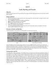
Intel 45nm Process Overview - UCSB CAD & Test
Intel 45nm Process Overview - UCSB CAD & Test
Intel 45nm Process Overview - UCSB CAD & Test
SHOW LESS

Create successful ePaper yourself
Turn your PDF publications into a flip-book with our unique Google optimized e-Paper software.
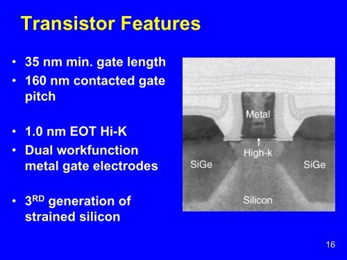
Transistor Features<br />
• 35 nm min. gate length<br />
• 160 nm contacted gate<br />
pitch<br />
• 1.0 nm EOT Hi-K<br />
• Dual workfunction<br />
metal gate electrodes<br />
• 3 RD generation of<br />
strained silicon<br />
16