Intel 45nm Process Overview - UCSB CAD & Test
Intel 45nm Process Overview - UCSB CAD & Test
Intel 45nm Process Overview - UCSB CAD & Test
Create successful ePaper yourself
Turn your PDF publications into a flip-book with our unique Google optimized e-Paper software.
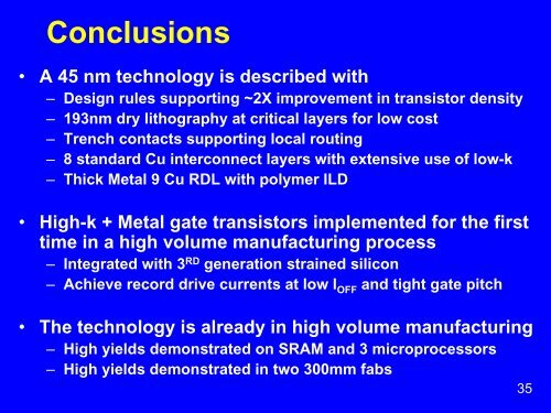
Conclusions<br />
• A 45 nm technology is described with<br />
– Design rules supporting ~2X improvement in transistor density<br />
– 193nm dry lithography at critical layers for low cost<br />
– Trench contacts supporting local routing<br />
– 8 standard Cu interconnect layers with extensive use of low-k<br />
– Thick Metal 9 Cu RDL with polymer ILD<br />
• High-k + Metal gate transistors implemented for the first<br />
time in a high volume manufacturing process<br />
– Integrated with 3 RD generation strained silicon<br />
– Achieve record drive currents at low I OFF and tight gate pitch<br />
• The technology is already in high volume manufacturing<br />
– High yields demonstrated on SRAM and 3 microprocessors<br />
– High yields demonstrated in two 300mm fabs<br />
35


