Intel 45nm Process Overview - UCSB CAD & Test
Intel 45nm Process Overview - UCSB CAD & Test
Intel 45nm Process Overview - UCSB CAD & Test
SHOW LESS

You also want an ePaper? Increase the reach of your titles
YUMPU automatically turns print PDFs into web optimized ePapers that Google loves.
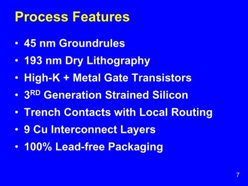
<strong>Process</strong> Features<br />
• 45 nm Groundrules<br />
• 193 nm Dry Lithography<br />
• High-K + Metal Gate Transistors<br />
• 3 RD Generation Strained Silicon<br />
• Trench Contacts with Local Routing<br />
• 9 Cu Interconnect Layers<br />
• 100% Lead-free Packaging<br />
7