Intel 45nm Process Overview - UCSB CAD & Test
Intel 45nm Process Overview - UCSB CAD & Test
Intel 45nm Process Overview - UCSB CAD & Test

Create successful ePaper yourself
Turn your PDF publications into a flip-book with our unique Google optimized e-Paper software.
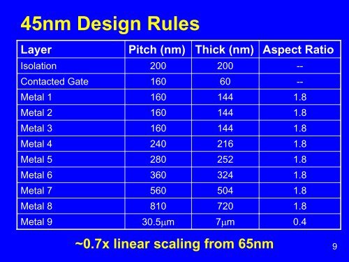
<strong>45nm</strong> Design Rules<br />
Layer Pitch (nm) Thick (nm) Aspect Ratio<br />
Isolation 200 200<br />
Contacted Gate 160 60<br />
--<br />
Metal 1 160 144<br />
1.8<br />
Metal 2 160 144<br />
1.8<br />
Metal 3 160 144<br />
1.8<br />
Metal 4 240 216<br />
1.8<br />
Metal 5 280 252<br />
1.8<br />
Metal 6 360 324<br />
1.8<br />
Metal 7 560 504 1.8<br />
Metal 8 810 720 1.8<br />
Metal 9 30.5μm 7μm<br />
0.4<br />
~0.7x linear scaling from 65nm<br />
--<br />
9