

Data Sheet - Freescale Semiconductor
Data Sheet - Freescale Semiconductor
Data Sheet - Freescale Semiconductor

You also want an ePaper? Increase the reach of your titles
YUMPU automatically turns print PDFs into web optimized ePapers that Google loves.
<strong>Freescale</strong> <strong>Semiconductor</strong> Document Number: MMA27XXW<br />
<strong>Data</strong> <strong>Sheet</strong>: Advance Information Rev. 0.5, 4/2013<br />
An Energy-Efficient Solution by <strong>Freescale</strong><br />
Xtrinsic MMA27XXW/17XXW DSI3<br />
Inertial Sensor<br />
MMA27XXW/17XXW family, a SafeAssure solution, includes the DSI3 compatible<br />
overdamped X-axis or Z-axis satellite accelerometers.<br />
Features<br />
• ±25 g, ±125 g, ±187 g, ±250 g, ±375 g, X-axis nominal full-scale range<br />
• ±250 g, Z-axis nominal full-scale range<br />
• DSI3 compatible<br />
— Discovery Mode for physical location identification<br />
— High-side bus switch output driver<br />
— Command and Response Mode support for device configuration<br />
— Periodic <strong>Data</strong> Collection Mode support for acceleration data transfers<br />
— Background Diagnostic Mode support during Periodic <strong>Data</strong> Collection<br />
Mode<br />
• -40°C to 125°C operating temperature range<br />
• 16 μs internal sample rate, with interpolation to 1 μs<br />
• Six selectable low-pass filter options from 180 Hz to 1200 Hz<br />
• Single-pole, IIR high-pass filter with fast startup and optional output rate limiting<br />
• Pb-Free, 16-pin QFN, 6 x 6 package<br />
Referenced Documents<br />
• DSI3 Standard Revision 1.0, Dated February 16, 2011<br />
• AEC-Q100, Revision G, dated May 14, 2007<br />
ORDERING INFORMATION<br />
Part Number Axis Range Package Shipping<br />
MMA2702W X ±25 g 2086-01 Rail<br />
MMA2712W X ±125 g 2086-01 Rail<br />
MMA2718W X ±187 g 2086-01 Rail<br />
MMA2725W X ±250 g 2086-01 Rail<br />
MMA2737W X ±375 g 2086-01 Rail<br />
MMA1725W Z ±250 g 2086-01 Rail<br />
MMA2702WR2 X ±25 g 2086-01 Tape & Reel<br />
MMA2712WR2 X ±125 g 2086-01 Tape & Reel<br />
MMA2718WR2 X ±187 g 2086-01 Tape & Reel<br />
MMA2725WR2 X ±250 g 2086-01 Tape & Reel<br />
MMA2737WR2 X ±375 g 2086-01 Tape & Reel<br />
MMA1725WR2 Z ±250 g 2086-01 Tape & Reel<br />
This document contains information on a new product. Specifications and information herein<br />
are subject to change without notice. <strong>Freescale</strong> reserves the right to change the detail<br />
© 2013 <strong>Freescale</strong> <strong>Semiconductor</strong>, Inc. All rights reserved.<br />
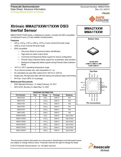
BUS_O<br />
NC<br />
BUS_I<br />
BUSRTN<br />
MMA27XXW<br />
MMA17XXW<br />
Bottom View<br />
16-PIN QFN<br />
6 MM X 6 MM X 2 MM<br />
CASE 2086-01<br />
1<br />
2<br />
3<br />
4<br />
BUSSW<br />
PCM<br />
Top View<br />
TEST<br />
TEST_SCLK<br />
TEST2<br />
TEST_MISO<br />
V BUF<br />
16 15 14 13<br />
17<br />
5 6 7 8<br />
TEST_MOSI<br />
Pin Connections<br />
12 VSS 11 VREGA 10 TEST_CS<br />
9 VREG
Contents<br />
1 Block Diagram, Pin Descriptions, Application Diagram, and Device Orientation . . . . . . . . . . . . . . . . . . . . . . . . . . . . 3<br />
1.1 Block diagram . . . . . . . . . . . . . . . . . . . . . . . . . . . . . . . . . . . . . . . . . . . . . . . . . . . . . . . . . . . . . . . . . . . . . . . . . . . . . . . 3<br />
1.2 Pin descriptions. . . . . . . . . . . . . . . . . . . . . . . . . . . . . . . . . . . . . . . . . . . . . . . . . . . . . . . . . . . . . . . . . . . . . . . . . . . . . . 4<br />
1.3 Application diagram . . . . . . . . . . . . . . . . . . . . . . . . . . . . . . . . . . . . . . . . . . . . . . . . . . . . . . . . . . . . . . . . . . . . . . . . . . 5<br />
1.4 Device orientation and device marking. . . . . . . . . . . . . . . . . . . . . . . . . . . . . . . . . . . . . . . . . . . . . . . . . . . . . . . . . . . . 6<br />
2 Electrical Characteristics . . . . . . . . . . . . . . . . . . . . . . . . . . . . . . . . . . . . . . . . . . . . . . . . . . . . . . . . . . . . . . . . . . . . . . . . . . 7<br />
2.1 Maximum ratings. . . . . . . . . . . . . . . . . . . . . . . . . . . . . . . . . . . . . . . . . . . . . . . . . . . . . . . . . . . . . . . . . . . . . . . . . . . . . 7<br />
2.2 Operating range . . . . . . . . . . . . . . . . . . . . . . . . . . . . . . . . . . . . . . . . . . . . . . . . . . . . . . . . . . . . . . . . . . . . . . . . . . . . . 7<br />
2.3 Electrical characteristics - supply and I/O . . . . . . . . . . . . . . . . . . . . . . . . . . . . . . . . . . . . . . . . . . . . . . . . . . . . . . . . . . 8<br />
2.4 Electrical Characteristics - sensor and signal chain . . . . . . . . . . . . . . . . . . . . . . . . . . . . . . . . . . . . . . . . . . . . . . . . . . 9<br />
2.5 Electrical characteristics - self-test and overload . . . . . . . . . . . . . . . . . . . . . . . . . . . . . . . . . . . . . . . . . . . . . . . . . . . 10<br />
2.6 Dynamic electrical characteristics - DSI3 . . . . . . . . . . . . . . . . . . . . . . . . . . . . . . . . . . . . . . . . . . . . . . . . . . . . . . . . . 11<br />
2.7 Dynamic electrical characteristics - signal chain. . . . . . . . . . . . . . . . . . . . . . . . . . . . . . . . . . . . . . . . . . . . . . . . . . . . 12<br />
2.8 Dynamic electrical characteristics - supply and support circuitry . . . . . . . . . . . . . . . . . . . . . . . . . . . . . . . . . . . . . . . 13<br />
3 Functional Description . . . . . . . . . . . . . . . . . . . . . . . . . . . . . . . . . . . . . . . . . . . . . . . . . . . . . . . . . . . . . . . . . . . . . . . . . . . 14<br />
3.1 User-accessible data array . . . . . . . . . . . . . . . . . . . . . . . . . . . . . . . . . . . . . . . . . . . . . . . . . . . . . . . . . . . . . . . . . . . . 14<br />
3.2 OTP and Read/Write register array CRC verification . . . . . . . . . . . . . . . . . . . . . . . . . . . . . . . . . . . . . . . . . . . . . . . . 31<br />
3.3 Voltage regulators. . . . . . . . . . . . . . . . . . . . . . . . . . . . . . . . . . . . . . . . . . . . . . . . . . . . . . . . . . . . . . . . . . . . . . . . . . . 33<br />
3.4 Internal oscillator. . . . . . . . . . . . . . . . . . . . . . . . . . . . . . . . . . . . . . . . . . . . . . . . . . . . . . . . . . . . . . . . . . . . . . . . . . . . 37<br />
3.5 Acceleration signal path . . . . . . . . . . . . . . . . . . . . . . . . . . . . . . . . . . . . . . . . . . . . . . . . . . . . . . . . . . . . . . . . . . . . . . 38<br />
3.6 DSI3 physical layer . . . . . . . . . . . . . . . . . . . . . . . . . . . . . . . . . . . . . . . . . . . . . . . . . . . . . . . . . . . . . . . . . . . . . . . . . . 55<br />
3.7 <strong>Data</strong> transmission modes . . . . . . . . . . . . . . . . . . . . . . . . . . . . . . . . . . . . . . . . . . . . . . . . . . . . . . . . . . . . . . . . . . . . . 58<br />
3.8 Initialization timing. . . . . . . . . . . . . . . . . . . . . . . . . . . . . . . . . . . . . . . . . . . . . . . . . . . . . . . . . . . . . . . . . . . . . . . . . . . 59<br />
3.9 Overload response . . . . . . . . . . . . . . . . . . . . . . . . . . . . . . . . . . . . . . . . . . . . . . . . . . . . . . . . . . . . . . . . . . . . . . . . . . 60<br />
4 DSI3 Protocol . . . . . . . . . . . . . . . . . . . . . . . . . . . . . . . . . . . . . . . . . . . . . . . . . . . . . . . . . . . . . . . . . . . . . . . . . . . . . . . . . . 61<br />
4.1 Address assignment . . . . . . . . . . . . . . . . . . . . . . . . . . . . . . . . . . . . . . . . . . . . . . . . . . . . . . . . . . . . . . . . . . . . . . . . . 61<br />
4.2 DSI3 Command and Response Mode . . . . . . . . . . . . . . . . . . . . . . . . . . . . . . . . . . . . . . . . . . . . . . . . . . . . . . . . . . . 62<br />
4.3 DSI3 Periodic <strong>Data</strong> Collection Mode and Background Diagnostic Mode . . . . . . . . . . . . . . . . . . . . . . . . . . . . . . . . . 72<br />
4.4 Maximum number of devices on a network . . . . . . . . . . . . . . . . . . . . . . . . . . . . . . . . . . . . . . . . . . . . . . . . . . . . . . . 77<br />
5 Exception Handling . . . . . . . . . . . . . . . . . . . . . . . . . . . . . . . . . . . . . . . . . . . . . . . . . . . . . . . . . . . . . . . . . . . . . . . . . . . . . 78<br />
6 Recommended Footprint . . . . . . . . . . . . . . . . . . . . . . . . . . . . . . . . . . . . . . . . . . . . . . . . . . . . . . . . . . . . . . . . . . . . . . . . . 79<br />
7 Package Dimensions . . . . . . . . . . . . . . . . . . . . . . . . . . . . . . . . . . . . . . . . . . . . . . . . . . . . . . . . . . . . . . . . . . . . . . . . . . . . 80<br />
8 Revision History . . . . . . . . . . . . . . . . . . . . . . . . . . . . . . . . . . . . . . . . . . . . . . . . . . . . . . . . . . . . . . . . . . . . . . . . . . . . . . . . 83<br />
Related Documentation<br />
The MMA27XXW and MMA17XXW devices features and operations are described in a variety of reference manuals, user guides,<br />
and application notes. To find the most-current versions of these documents:<br />
1. Go to the <strong>Freescale</strong> homepage at:<br />
MMA27XXW<br />
http://www.freescale.com/<br />
2. In the Keyword search box at the top of the page, enter the device number MMA27XXW or MMA17XXW.<br />
3. In the Refine Your Result pane on the left, click on the Documentation link.<br />
Sensors<br />
2 <strong>Freescale</strong> <strong>Semiconductor</strong>, Inc.
1 Block Diagram, Pin Descriptions, Application Diagram, and Device<br />
Orientation<br />
1.1 Block diagram<br />
BUS_I<br />
BUSRTN<br />
BUS_O<br />
BUSSW<br />
Self-test<br />
Interface<br />
g-cell<br />
BUS_I<br />
R SENSE<br />
V REGA<br />
Buffer<br />
Voltage<br />
Regulator<br />
Reference<br />
Voltage<br />
DSI3 Command<br />
Decoder<br />
NVM Programming<br />
Interface<br />
ΣΔ<br />
Converter<br />
Serial<br />
Encoder<br />
Daisy-Chain<br />
Switch Driver<br />
V REG<br />
V REG<br />
V BUF<br />
V REF<br />
Sinc filter<br />
Control<br />
Logic<br />
CONTROL<br />
IN<br />
Digital<br />
Gain<br />
Internal<br />
Voltage<br />
Regulator<br />
SIGNAL<br />
OUT<br />
Figure 1. Internal block diagram<br />
V REGA<br />
MMA27XXW<br />
Sensors<br />
<strong>Freescale</strong> <strong>Semiconductor</strong>, Inc. 3<br />
IIR<br />
LPF<br />
V REG<br />
V BUF<br />
Oscillator<br />
OTP<br />
Array<br />
DSP<br />
Compensation<br />
Low Voltage<br />
Detection<br />
SPI<br />
PCM<br />
Encoder<br />
Offset<br />
Monitor<br />
HPF<br />
V BUF<br />
V REG<br />
V REGA<br />
V SS<br />
TEST_CS<br />
TEST_SCLK<br />
TEST_MOSI<br />
TEST_MISO<br />
PCM<br />
Interpolation
1.2 Pin descriptions<br />
Table 1. Pin descriptions<br />
MMA27XXW<br />
Figure 2. Pin connections<br />
Pin Pin name Formal name Definition<br />
1 BUS_O Supply out<br />
This pin is connected to the BUS_I pin through an internal sense resistor and provides the supply<br />
connection to the next slave in a daisy-chain configuration. An external capacitor must be connected<br />
between this pin and V SS. Reference Figure 3.<br />
2 NC Not connected This pin is not internally connected and must be left unconnected or tied to V SS in the application.<br />
3 BUS_I<br />
Supply and<br />
communication<br />
This pin is connected to the DSI supply line and supplies power to the device. An external capacitor must<br />
be connected between this pin and BUSRTN. Reference Figure 3.<br />
4 BUSRTN Supply return This pin is the DSI supply return node.<br />
5 PCM<br />
Pulse code<br />
modulated output<br />
6 TEST_SCLK SPI clock<br />
7 TEST_MISO SPI data out<br />
8 TEST_MOSI SPI data in<br />
9 V REG<br />
Internal<br />
supply<br />
10 TEST_CS Chip select<br />
11 V REGA<br />
12 V SS<br />
Internal<br />
supply<br />
Internal supply<br />
return<br />
13 V BUF Power supply<br />
BUS_O<br />
NC<br />
BUS_I<br />
BUSRTN<br />
1<br />
2<br />
3<br />
4<br />
BUSSW<br />
PCM<br />
TEST<br />
TEST_SCLK<br />
TEST2<br />
TEST_MISO<br />
If the PCM output is enabled, this pin provides a 4 MHz PCM signal proportional to the acceleration data<br />
for test purposes. If PCM is unused, this pin must be left unconnected.<br />
This input pin provides the serial clock to the SPI port for test purposes. An internal pull-down device is<br />
connected to this pin. This pin must be grounded or left unconnected in the application.<br />
This pin functions as the serial data output from the SPI port for test purposes. This pin must be left<br />
unconnected in the application.<br />
This pin functions as the serial data input to the SPI port for test purposes. An internal pull-down device<br />
is connected to this pin. This pin must be grounded or left unconnected in the application.<br />
This pin is connected to the power supply for the internal circuitry. An external capacitor must be<br />
connected between this pin and VSS. Reference Figure 3.<br />
This input pin provides the chip select to the SPI port for test purposes. An internal pullup device is<br />
connected to this pin. This pin must be left unconnected in the application.<br />
This pin is connected to the power supply for the internal circuitry. An external capacitor must be<br />
connected between this pin and VSSA . Reference Figure 3.<br />
This pin is the power supply return node for the internal power supplies and must be connected to<br />
BUSRTN in this application.<br />
This pin is connected to a buffer regulator for the internal circuitry. The buffer regulator supplies the<br />
internal regulators to provide immunity from EMC and supply dropouts. An external capacitor must be<br />
connected between this pin and VSS . Reference Figure 3.<br />
14 TEST2 Test pin This pin is must be connected to VSS in the application.<br />
15 TEST Test pin This pin is must be connected to VSS in the application.<br />
This pin is the drive for a high-side, daisy-chain switch. When switch is connected, daisy-chain mode is<br />
16 BUSSW<br />
Bus switch gate<br />
drive<br />
used, this pin is connected to the gate of a p-channel FET which connects BUS_I to the next slave in the<br />
daisy chain. An external pullup resistor is required on the gate of the p-channel FET. Reference<br />
Section 3.6.4. If unused, this pin must be left unconnected.<br />
17 PAD Die attach pad<br />
This pin is the die attach flag, and is internally connected to VSS . Reference Section 6 for die attach pad<br />
connection details.<br />
Corner pads Corner pads The corner pads are internally connected to VSS. Sensors<br />
4 <strong>Freescale</strong> <strong>Semiconductor</strong>, Inc.<br />
V BUF<br />
16 15 14 13<br />
17<br />
5 6 7 8<br />
TEST_MOSI<br />
12<br />
11<br />
10<br />
9<br />
V SS<br />
VREGA TEST_CS<br />
V REG
1.3 Application diagram<br />
C2 C3<br />
C4<br />
Table 2. External component recommendations<br />
VBUF BUS_I<br />
VREG V REGA<br />
V SS<br />
BUSRTN<br />
BUS_O<br />
BUSSW<br />
BUS_I<br />
BUS_I<br />
Figure 3. MMA27XXW/17XXW application diagram<br />
Ref Des Type Description Purpose<br />
BUSIN EMC and ESD protection. Capacitor value is dependent<br />
C1 Ceramic 220 pF, 10%, 50 V minimum, X7R on the DSI3 master device and must be chosen by the system<br />
implementer.<br />
C2 Ceramic 1 μF, 10%, 10 V minimum, X7R Voltage regulator output capacitor<br />
C3 Ceramic 1 μF, 10%, 10 V minimum, X7R Voltage regulator output capacitor<br />
C4 Ceramic 1 μF, 10%, 10 V minimum, X7R Voltage regulator output capacitor<br />
C5 Ceramic 100 pF, 10%, 50 V minimum, X7R BUSOUT EMC and ESD protection<br />
C6 Ceramic 100 pF, 10%, 50 V minimum, X7R BUSOUT EMC and ESD protection<br />
R1 General purpose 100 kΩ, 5%, 200 PPM Pullup resistor for external high-side, daisy-chain FET<br />
M1 P-channel MOSFET High-side, daisy-chain transistor<br />
D1 Zener diode MMBZ27Vxxxx or equivalent ESD protection diode<br />
MMA27XXW<br />
Sensors<br />
<strong>Freescale</strong> <strong>Semiconductor</strong>, Inc. 5<br />
C1<br />
R1<br />
Optional for<br />
Daisy Chain<br />
Optional for ESD<br />
D1<br />
C5<br />
C6<br />
M1<br />
BUSIN<br />
BUSRTN<br />
BUSOUT<br />
BUSOUT DC
1.4 Device orientation and device marking<br />
xxxxxxx<br />
xxxxxxx<br />
MMA27XXW<br />
xxxxxxx<br />
xxxxxxx<br />
X: 0 g<br />
X: +1 g X: 0 g X: -1 g X: 0 g X: 0 g<br />
Z: 0 g Z: 0 g Z: 0 g Z: 0 g Z: +1 g Z: -1 g<br />
MMAx7xxW<br />
AWLYWWZ<br />
xxxxxxx<br />
xxxxxxx<br />
xxxxxxx<br />
xxxxxxx<br />
EARTH GROUND<br />
Figure 4. Device orientation diagram<br />
<strong>Data</strong> Code Legend:<br />
A: Assembly Location<br />
WL: Wafer Lot Number (g-cell Lot Number)<br />
Y: Year<br />
WW: Work Week<br />
Z: Assembly Lot Number<br />
Figure 5. Device marking<br />
Sensors<br />
6 <strong>Freescale</strong> <strong>Semiconductor</strong>, Inc.
2 Electrical Characteristics<br />
2.1 Maximum ratings<br />
Maximum ratings are the extreme limits to which the device can be exposed without permanently damaging it.<br />
1<br />
2<br />
3<br />
4<br />
# Rating Symbol Value Unit<br />
Supply voltage (BUS_I, BUS_O, BUSSW)<br />
Reverse current ≤ 160 mA, t ≤ 80 ms<br />
Continuous<br />
Transient (< 10 us)<br />
2.2 Operating range<br />
BUS_I _REV<br />
BUS_I _MAX<br />
BUS_I _TRANS<br />
5 VBUF -0.3 to +4.0 V (6)<br />
6 VREG, VREGA, TEST_SCLK, TEST_CS, TEST_MOSI, TEST_MISO, PCM -0.3 to +3.0 V (6)<br />
7<br />
8<br />
9<br />
BUS_I, BUS_O and BUSRTN current<br />
Maximum duration 560 μs, with 10 ms repetition rate<br />
Continuous<br />
10 Powered shock (six sides, 0.5 ms duration) gpms ±2000 g (5)<br />
11 Unpowered shock (six sides, 0.5 ms duration) gshock ±2000 g (5)<br />
12 Drop shock (to concrete, tile or steel surface, 10 drops, any orientation) hDROP 1.2 m (5)<br />
13<br />
14<br />
15<br />
16<br />
17<br />
18<br />
19<br />
20<br />
21<br />
V BUS_I_L ≤ (V BUS_I - V SS ) ≤ V BUS_I_H , T L ≤ T A ≤ T H , ΔT ≤ 12°C/min, unless otherwise specified.<br />
MMA27XXW<br />
Sensors<br />
<strong>Freescale</strong> <strong>Semiconductor</strong>, Inc. 7<br />
I IN<br />
I IN<br />
-0.7<br />
+20.0<br />
+25.0<br />
Electrostatic discharge (per AEC-Q100), external pins<br />
BUS_I, BUS_O , BUSRTN, HBM (100 pF, 1.5 kΩ) V ESD ±4000 V (5)<br />
Electrostatic discharge (per AEC-Q100)<br />
HBM (100 pF, 1.5 kΩ)<br />
CDM (R = 0 Ω)<br />
MM (200 pF, 0 Ω)<br />
Temperature range<br />
Storage<br />
Junction<br />
V ESD<br />
V ESD<br />
V ESD<br />
T stg<br />
T J<br />
200<br />
150<br />
±2000<br />
±500<br />
±200<br />
-40 to +125<br />
-40 to +150<br />
22 Thermal resistance θ JC 2.5 °C/W (9,11)<br />
# Characteristic Symbol Min Typ Max Units<br />
23<br />
24<br />
25<br />
26<br />
27<br />
Supply voltage (measured at BUS_I pin)<br />
V HIGH<br />
V LOW rising<br />
V LOW falling<br />
Supply voltage (undervoltage)<br />
*<br />
*<br />
V BUS_I_HIGH_max<br />
V BUS_I_LOW_Rise<br />
V BUS_I_LOW_Fall<br />
V BUS_I_UV<br />
—<br />
4.5<br />
4.0<br />
VBUS_I_UV_F —<br />
—<br />
—<br />
—<br />
20.0<br />
—<br />
—<br />
VBUS_I_LOW_Fall 28 Programming voltage (I RD ≤ 85 mA)<br />
Applied to BUS_I VPP 14.0 — V BUS_I_HIGH_max V (6)<br />
29<br />
30<br />
31<br />
32<br />
33<br />
34<br />
ESD operating voltage<br />
(No device reset, C BUS_IN = 220 pF, D1 = MMBZ27Vxxxx)<br />
Maximum ±15 kV air discharge, 330 pF, 2.0 kΩ VBUS_I_ESD — — 12.0 V (9)<br />
Operating temperature range<br />
T A<br />
T A<br />
T L<br />
-40<br />
-40<br />
—<br />
—<br />
T H<br />
+105<br />
+125<br />
V<br />
V<br />
V<br />
mA<br />
mA<br />
V<br />
V<br />
V<br />
°C<br />
°C<br />
V<br />
V<br />
V<br />
V<br />
°C<br />
°C<br />
(6)<br />
(6)<br />
(9)<br />
(6)<br />
(6)<br />
(5)<br />
(5)<br />
(5)<br />
(5)<br />
(9)<br />
(1,6)<br />
(9)<br />
(1)<br />
(3,6)<br />
(1)<br />
(5,6)
2.3 Electrical characteristics - supply and I/O<br />
V BUS_I_L ≤ (V BUS_I - V SS) ≤ V BUS_I_H, T L ≤ T A ≤ T H, ΔT ≤ 12 °C/min, unless otherwise specified.<br />
# Characteristic Symbol Min Typ Max Units<br />
35<br />
36<br />
37<br />
Quiescent supply current<br />
V BUS_I = 4 V, V BUS_I = 20 V * I q 4.0 — 8.0 mA (1)<br />
Response current<br />
Low<br />
High<br />
MMA27XXW<br />
*<br />
*<br />
IRESP 2*IRESP I q+ 10.50<br />
I q+ 21.0<br />
I q+ 12.0<br />
I q+ 24.0<br />
I q+ 13.5<br />
I q+ 27.0<br />
38 V BUF current limit I INRUSH_MAX — — 30 mA (6)<br />
39<br />
40<br />
41<br />
42<br />
43<br />
44<br />
45<br />
46<br />
47<br />
48<br />
49<br />
50<br />
51<br />
52<br />
53<br />
54<br />
55<br />
56<br />
Internally regulated voltages<br />
V BUF, V BUS_I = 4 V, V BUS_I = 20 V<br />
V REG , V BUS_I = 4 V<br />
V REGA, V BUS_I = 4 V, V BUS_I = 20 V *<br />
Low-voltage detection threshold<br />
BUS_I falling<br />
V BUF falling<br />
V REG falling<br />
V REGA falling<br />
Low-voltage detection hysteresis<br />
External capacitor (V BUF, V REG, V REGA)<br />
Capacitance<br />
ESR (including interconnect resistance)<br />
V LOW detection threshold (Section 3.6.1)<br />
V LOW detection threshold<br />
V LOW detection hysteresis<br />
Discovery Mode current sense (Section 3.6.3)<br />
Sense resistor<br />
I RESP detection threshold (I BUS_O_q ≤ 24 mA)<br />
*<br />
*<br />
V BUF<br />
V REG<br />
V REGA<br />
V BUS_I_UV_F<br />
V BUF_UV_F<br />
V REG_UV_F<br />
V REGA_UV_F<br />
V HYST<br />
C VBUF , C VREG , C VREGA<br />
ESR<br />
V DELTA_THRESH<br />
V DELTA_THRESH_Hyst<br />
RSENSE IRESP_Det, VIRESP_Offset Sensors<br />
8 <strong>Freescale</strong> <strong>Semiconductor</strong>, Inc.<br />
3.250<br />
2.400<br />
2.425<br />
3.60<br />
2.80<br />
2.15<br />
2.15<br />
0.04<br />
500<br />
0<br />
V HIGH -1.25<br />
40<br />
3.400<br />
2.500<br />
2.500<br />
3.75<br />
3.05<br />
2.25<br />
2.25<br />
—<br />
1000<br />
—<br />
V HIGH -1.0<br />
60<br />
3.550<br />
2.600<br />
2.575<br />
3.90<br />
3.20<br />
2.35<br />
2.35<br />
—<br />
1500<br />
200<br />
V HIGH -0.75<br />
80<br />
Bus switch output low voltage (Section 3.6.4)<br />
I Load = 100 μA V BUS_SW_OL 0.0 — 0.45 V (3,6)<br />
Bus switch open drain output leakage current (BUSSW)<br />
V BUSSW = 20 V I BUS_SW_ODL — — 10 μA (3,6)<br />
Output high voltage (PCM)<br />
I Load = -100 μA V OH V REG - 0.1 — — V (3)<br />
Output low voltage (PCM)<br />
I Load = 100 μA V OL — — 0.1 V (3)<br />
1.3<br />
6<br />
2.15<br />
12<br />
3<br />
18<br />
mA<br />
mA<br />
V<br />
V<br />
V<br />
V<br />
V<br />
V<br />
V<br />
V<br />
nF<br />
mΩ<br />
V<br />
mV<br />
Ω<br />
mA<br />
(1)<br />
(1)<br />
(1)<br />
(1)<br />
(1)<br />
(3,6)<br />
(3,6)<br />
(3,6)<br />
(3,6)<br />
(6)<br />
(9)<br />
(9)<br />
(3,6)<br />
(6)<br />
(6)<br />
(3,6)
2.4 Electrical Characteristics - sensor and signal chain<br />
V BUS_I_L ≤ (V BUS_I - V SS) ≤ V BUS_I_H, T L ≤ T A ≤ T H, ΔT ≤ 12 °C/min, unless otherwise specified.<br />
57<br />
58<br />
59<br />
60<br />
61<br />
62<br />
63<br />
64<br />
65<br />
66<br />
# Characteristic Symbol Min Typ Max Units<br />
Sensitivity (T A = 25°C, 10-bit output @ 100 Hz, referenced to 0Hz: ±5%)<br />
±25 g range<br />
±125 g range<br />
±187 g range<br />
±250 g range<br />
±375 g range<br />
Sensitivity (T L ≤ T A ≤ T H, V BUS_I_UV_F ≤ V BUS_I ≤ V LOW<br />
10-bit output @ 100 Hz, referenced to 0 Hz: ±7%)<br />
±25 g range<br />
±125 g range<br />
±187 g range<br />
±250 g range<br />
±375 g range<br />
MMA27XXW<br />
Sensors<br />
<strong>Freescale</strong> <strong>Semiconductor</strong>, Inc. 9<br />
*<br />
*<br />
*<br />
*<br />
*<br />
*<br />
*<br />
*<br />
*<br />
*<br />
SENS 025<br />
SENS 125<br />
SENS 187<br />
SENS 250<br />
SENS 375<br />
SENS 025<br />
SENS 125<br />
SENS 187<br />
SENS 250<br />
SENS 375<br />
19.456<br />
3.8912<br />
2.5944<br />
1.9456<br />
1.2967<br />
19.046<br />
3.8092<br />
2.5398<br />
1.9046<br />
1.2694<br />
20.480<br />
4.0960<br />
2.7310<br />
2.0480<br />
1.3650<br />
20.480<br />
4.0960<br />
2.7310<br />
2.0480<br />
1.3650<br />
21.504<br />
4.3008<br />
2.8676<br />
2.1504<br />
1.4333<br />
21.914<br />
4.3828<br />
2.9222<br />
2.1914<br />
1.4606<br />
LSB/g<br />
LSB/g<br />
LSB/g<br />
LSB/g<br />
LSB/g<br />
LSB/g<br />
LSB/g<br />
LSB/g<br />
LSB/g<br />
LSB/g<br />
67<br />
Digital offset before offset cancellation (10-bit)<br />
±25 g, ±125 g, ±250 g Z-axis<br />
* OFF10Bit -100 0 +100 LSB (1)<br />
68 VBUS_I_UV_F ≤ VBUS_I ≤ VLOW, ±25 g, ±125 g, ±250 g Z-axis<br />
OFF10Bit -100 0 +100 LSB (6)<br />
69 ±187 g, ±250 g X-axis, ±375 g<br />
* OFF10Bit -52 0 +52 LSB (1)<br />
70 VBUS_I_UV_F ≤ VBUS_I ≤ VLOW , ±187 g, ±250 g X-axis, ±375 g<br />
OFF10Bit -52 0 +52 LSB (6)<br />
71 Digital offset after offset cancellation (10-bit, all filter options) OFF10Bit -1 0 +1 LSB (6,8,9)<br />
72<br />
73<br />
74<br />
75<br />
76<br />
77<br />
78<br />
79<br />
80<br />
81<br />
82<br />
83<br />
84<br />
Continuous offset monitor limit<br />
10-bit output, before compensation, ±25 g<br />
10-bit output, before compensation, ±125 g, ±250 g Z-axis<br />
10-bit output, before compensation, ±187 g, ±250 g X-axis, ±375 g<br />
Range of output (10-bit mode)<br />
Acceleration (signed)<br />
Acceleration (unsigned)<br />
Error code (signed)<br />
Error code (unsigned)<br />
Cross-axis sensitivity<br />
Z-axis to X-axis<br />
Y-axis to X-axis<br />
X-axis to Z-axis<br />
Y-axis to Z-axis<br />
System output noise peak (peak value of 100 samples @ 2 kHz)<br />
10-bit mode, LPF = 180 Hz, 2-Pole, All Ranges<br />
10-bit mode, LPF = 400 Hz, 4-Pole, All Ranges<br />
OFF MON<br />
OFF MON<br />
OFF MON<br />
RANGE Signed<br />
RANGE Unsigned<br />
ERR Signed<br />
ERR Unsigned<br />
V ZX<br />
V YX<br />
V XZ<br />
V YZ<br />
n Peak_180<br />
n Peak_400<br />
85<br />
86<br />
System output noise average (average value of 100 samples @ 2 kHz)<br />
10-bit mode, LPF = 180 Hz, 2-pole, all ranges<br />
10-bit mode, LPF = 400 Hz, 4-pole, all ranges<br />
*<br />
*<br />
nRMS_180 nRMS_400 —<br />
—<br />
—<br />
—<br />
+1.0<br />
+1.0<br />
LSB<br />
LSB<br />
(1)<br />
(6)<br />
87 Nonlinearity (10-bit output, all ranges) NLOUT -2 — +2 % (6)<br />
-150<br />
-120<br />
-70<br />
-511<br />
1<br />
—<br />
—<br />
-5<br />
-5<br />
-5<br />
-5<br />
-3<br />
-4<br />
—<br />
—<br />
—<br />
—<br />
—<br />
-512<br />
0<br />
—<br />
—<br />
—<br />
—<br />
—<br />
—<br />
+150<br />
+120<br />
+70<br />
+511<br />
1023<br />
—<br />
—<br />
+5<br />
+5<br />
+5<br />
+5<br />
+3<br />
+4<br />
LSB<br />
LSB<br />
LSB<br />
LSB<br />
LSB<br />
LSB<br />
LSB<br />
%<br />
%<br />
%<br />
%<br />
LSB<br />
LSB<br />
(1)<br />
(1)<br />
(1)<br />
(1)<br />
(1)<br />
(1)<br />
(1)<br />
(1)<br />
(1)<br />
(1)<br />
(7,8)<br />
(7,8)<br />
(7,8)<br />
(7,8)<br />
(7,9)<br />
(7,8)<br />
(7,9)<br />
(6)<br />
(6)<br />
(6)<br />
(6)<br />
(1)<br />
(6)
2.5 Electrical characteristics - self-test and overload<br />
V BUS_I_L ≤ (V BUS_I - V SS) ≤ V BUS_I_H, T L ≤ T A ≤ T H, ΔT ≤ 12°C/min, unless otherwise specified.<br />
88<br />
89<br />
90<br />
91<br />
92<br />
93<br />
94<br />
95<br />
96<br />
97<br />
98<br />
# Characteristic Symbol Min Typ Max Units<br />
99<br />
100<br />
101<br />
102<br />
103<br />
104<br />
105<br />
10-bit output during active self-test<br />
±25 g range, X-axis<br />
±125 g range, X-axis<br />
±187 g range, X-axis<br />
±250 g range, X-axis<br />
±375 g range, X-axis<br />
±250 g range, Z-axis<br />
MMA27XXW<br />
Sensors<br />
10 <strong>Freescale</strong> <strong>Semiconductor</strong>, Inc.<br />
*<br />
*<br />
*<br />
*<br />
*<br />
*<br />
g ST10_25X<br />
g ST10_125X<br />
g ST10_187X<br />
g ST10_250X<br />
g ST10_375X<br />
g ST10_250Z<br />
ΔST MIN<br />
124<br />
236<br />
156<br />
117<br />
77<br />
80<br />
ΔST NOM<br />
—<br />
—<br />
—<br />
—<br />
—<br />
—<br />
ΔST MAX<br />
208<br />
395<br />
263<br />
198<br />
131<br />
160<br />
Self-test accuracy: Δ from stored value, including sensitivity error<br />
-40°C ≤ T A ≤ 125°C (Section 3.5.2) * ΔSTACC -10 — +10 % (1,5)<br />
Transducer clipping limit<br />
±25 g, X-axis, positive/negative<br />
±125 g, ±187 g, ±250 g, ±375 g, X-axis, positive/negative<br />
±250 g, Z-axis positive<br />
±250 g, Z-axis negative<br />
Sinc filter clipping limit<br />
±25 g, X-axis, positive/negative (MMA2702WR2)<br />
±125 g, X-axis, positive/negative (MMA2712WR2)<br />
±187 g, X-axis positive/negative (MMA2718WR2)<br />
±250 g, X-axis positive/negative (MMA2725WR2)<br />
±375 g, X-axis positive/negative (MMA2737WR2)<br />
±250 g, Z-axis, positive (MMA1725WR2)<br />
±250 g, Z-axis, negative (MMA1725WR2)<br />
g g-cell_ClipLowX<br />
g g-cell_ClipHiX<br />
g g-cell_ClipHiZP<br />
g g-cell_ClipHiZN<br />
g ADC_Clip_25X_H<br />
g ADC_Clip_125X_H<br />
g ADC_Clip_187X_H<br />
g ADC_Clip_250X_H<br />
g ADC_Clip_375X_H<br />
g ADC_Clip_250ZPH<br />
g ADC_Clip_250ZNH<br />
400<br />
1700<br />
2200<br />
-3700<br />
190<br />
920<br />
1600<br />
1600<br />
1600<br />
1500<br />
-3200<br />
470<br />
2100<br />
2700<br />
-3200<br />
210<br />
1100<br />
1900<br />
1900<br />
1900<br />
2000<br />
-2900<br />
500<br />
2300<br />
3300<br />
-2700<br />
240<br />
1300<br />
2200<br />
2200<br />
2200<br />
2500<br />
-2500<br />
LSB<br />
LSB<br />
LSB<br />
LSB<br />
LSB<br />
LSB<br />
g<br />
g<br />
g<br />
g<br />
g<br />
g<br />
g<br />
g<br />
g<br />
g<br />
g<br />
(1)<br />
(1)<br />
(1)<br />
(1)<br />
(1)<br />
(1)<br />
(9)<br />
(9)<br />
(9)<br />
(9)<br />
(9)<br />
(9)<br />
(9)<br />
(9)<br />
(9)<br />
(9)<br />
(9)
2.6 Dynamic electrical characteristics - DSI3<br />
V BUS_I_L ≤ (V BUS_I - V SS) ≤ V BUS_I_H, T L ≤ T A ≤ T H, ΔT ≤ 12°C/min, unless otherwise specified.<br />
# Characteristic Symbol Min Typ Max Units<br />
106<br />
107<br />
108<br />
109<br />
110<br />
111<br />
112<br />
113<br />
114<br />
115<br />
116<br />
117<br />
118<br />
119<br />
120<br />
121<br />
122<br />
123<br />
124<br />
125<br />
126<br />
127<br />
128<br />
129<br />
130<br />
131<br />
132<br />
133<br />
134<br />
135<br />
136<br />
137<br />
138<br />
139<br />
140<br />
141<br />
142<br />
143<br />
144<br />
145<br />
146<br />
147<br />
Reset recovery (all modes, excluding VBUS_I voltage ramp time)<br />
POR to 1st command (Section 3.6)<br />
POR to acceleration data ready (Section 3.6)<br />
Command reception (general)<br />
VHIGH low-pass filter time constant (Section 3.6.1)<br />
VHIGH detection analog delay (Section 3.6.1)<br />
iq low-pass filter time constant (Section 3.6.3)<br />
Command valid time (Section 3.6.1)<br />
Response transmission (general, Section 4.2.3)<br />
Response slew time: 2.0 mA to 10.0 mA, 10.0 mA to 2.0 mA<br />
Response slew time: 4.0 mA to 20.0 mA, 20.0 mA to 4.0 mA<br />
tSLEW1_RESP- tSLEW2_RESP tSLEW1_RESP_Rise- tSLEW2_RESP_Fall Response current activation time: current activated to 50%<br />
Command reception (Discovery Mode)<br />
Command start time (Section 4.1)<br />
Command bit time (Section 4.1)<br />
Command transmission period (Section 4.1)<br />
Command blocking time, Discovery Mode (Section 3.6.1)<br />
ICCQ sample delay time (Section 3.6.3)<br />
ICCQ sample time (Section 3.6.3)<br />
IDISC sample delay time (Section 3.6.3)<br />
IDISC sample time (Section 3.6.3)<br />
Response transmission (Discovery Mode)<br />
Response start delay (Section 4.1)<br />
Response ramp time (Section 4.1)<br />
Response ramp rate (Section 4.1)<br />
Response idle time (Section 4.1)<br />
Response peak current (Section 4.1)<br />
Command reception (Command and Response Mode)<br />
Command bit time (Section 4.2)<br />
Command transmission period (Section 4.2)<br />
Command blocking time, CRM (Section 3.6.1)<br />
Command blocking start time, CRM (Section 3.6.1)<br />
Response transmission (Command and Response Mode)<br />
Response chip time<br />
Response start time (Section 4.2)<br />
Command reception (Periodic <strong>Data</strong> Collection Mode)<br />
Command bit time (Section 4.3)<br />
Command transmission period (Section 4.3)<br />
Command transmission period resolution<br />
Command blocking time, PDCM (Section 4.3.2)<br />
Command blocking time resolution, PDCM (Section 4.3.2)<br />
Command blocking start time, PDCM (Section 4.3.2)<br />
Command blocking start time, BDM command<br />
Response transmission (Periodic <strong>Data</strong> Collection Mode)<br />
Response chip time typical (Section 3.1.15.3)<br />
Response chip resolution (Section 3.1.15.3)<br />
Response start time typical (Section 4.3)<br />
Response start time typical, BDM enabled (Section 4.3)<br />
Response start time resolution<br />
t DSI_POR<br />
t DSP_POR<br />
t VHIGH_RC<br />
t VHIGH_Delay<br />
t IQ_RC<br />
t Cmd_Valid<br />
t SLEW1_RESP<br />
t SLEW2_RESP<br />
Δt SLEW<br />
Δt SLEW_rf<br />
t ACT_RESP<br />
t START_DISC<br />
t DISC_BitTime<br />
t PER_DISC<br />
t CmdBlock_DISC<br />
t Disc_Dly<br />
t Disc_Iccqsamp<br />
t IDiscsamp_Dly<br />
t IDiscsamp<br />
t START_DISC_RSP<br />
t DISC_Ramp_RSP<br />
I DISC_Ramp<br />
t DISC_Idle_RSP<br />
I DISC_Peak<br />
t Cmd_BitTime<br />
t PER_CRM<br />
t CmdBlock_CRM<br />
t CmdBlock_ST_CRM<br />
t CHIP_CRM<br />
t START_CRM<br />
t Cmd_BitTime<br />
t PER_PDCM<br />
t PER_PDCM_Res<br />
t CmdBlock_PDCM<br />
t CmdBlockRes_PDCM<br />
t CmdBlock_ST_PDCM<br />
t CmdBlock_ST_BDM<br />
t CHIP_PDCM<br />
t CHIPRes_PDCM<br />
t START_PDCM<br />
t START_PDCM_BDM<br />
t ST_RES_PDCM<br />
MMA27XXW<br />
Sensors<br />
<strong>Freescale</strong> <strong>Semiconductor</strong>, Inc. 11<br />
—<br />
—<br />
60<br />
—<br />
200<br />
—<br />
200<br />
200<br />
-100<br />
-250<br />
200<br />
t DSI_POR<br />
—<br />
1000/f OSC<br />
—<br />
—<br />
—<br />
—<br />
—<br />
—<br />
—<br />
—<br />
—<br />
—<br />
—<br />
tPER_PDCM —<br />
—<br />
—<br />
—<br />
5<br />
tDSI_POR 120<br />
—<br />
400<br />
2<br />
400<br />
400<br />
—<br />
—<br />
—<br />
—<br />
16<br />
—<br />
96<br />
48<br />
15<br />
65<br />
31<br />
64<br />
16<br />
1.5<br />
16<br />
2*I RESP<br />
8<br />
—<br />
456<br />
268<br />
5<br />
295<br />
—<br />
—<br />
180<br />
600<br />
600<br />
—<br />
600<br />
600<br />
100<br />
250<br />
400<br />
12<br />
—<br />
—<br />
—<br />
—<br />
—<br />
—<br />
—<br />
—<br />
—<br />
—<br />
—<br />
—<br />
—<br />
8 x tPER_PDCM —<br />
—<br />
—<br />
—<br />
ms<br />
s<br />
μs<br />
ns<br />
μs<br />
μs<br />
ns<br />
ns<br />
ns<br />
ns<br />
ns<br />
ms<br />
μs<br />
s<br />
μs<br />
μs<br />
μs<br />
μs<br />
μs<br />
μs<br />
μs<br />
mA/μs<br />
μs<br />
mA<br />
148<br />
Response transmission (Background Diagnostic Mode)<br />
Response start time (Section 4.3) tSTART_BDM — 20 — μs (7,8)<br />
149 Register write to BUSSW active tBS — 456 — μs (7,8)<br />
150 DSI data latency<br />
OTP program timing<br />
tLAT_DSI — 0.5 6.25 μs (7,9)<br />
151 Time to program the user OTP array tNVM_WRITE_MAX — — 60 ms (7,8)<br />
—<br />
100<br />
—<br />
1<br />
—<br />
—<br />
—<br />
3<br />
—<br />
20<br />
44<br />
—<br />
8<br />
—<br />
5<br />
—<br />
1<br />
20<br />
44<br />
—<br />
0.5<br />
—<br />
—<br />
1<br />
—<br />
5000<br />
—<br />
4095<br />
—<br />
—<br />
—<br />
6.5<br />
—<br />
4095<br />
4095<br />
—<br />
μs<br />
s<br />
μs<br />
μs<br />
μs<br />
μs<br />
μs<br />
μs<br />
μs<br />
μs<br />
μs<br />
μs<br />
μs<br />
μs<br />
μs<br />
μs<br />
μs<br />
μs<br />
(7,8)<br />
(7,8)<br />
(8,9)<br />
(8,9)<br />
(8,9)<br />
(7,9)<br />
(6,8)<br />
(6,8)<br />
(8,9)<br />
(8,9)<br />
(8,9)<br />
(7,8)<br />
(7,8)<br />
(7,8)<br />
(7,8)<br />
(7,9)<br />
(7,9)<br />
(7,9)<br />
(7,9)<br />
(7,8)<br />
(7,8)<br />
(6,8)<br />
(7,8)<br />
(6,8)<br />
(7,8)<br />
(7,8)<br />
(7,8)<br />
(7,8)<br />
(7,8)<br />
(7,8)<br />
(7,8)<br />
(7,8)<br />
(7,8)<br />
(7,8)<br />
(7,8)<br />
(7,8)<br />
(7,8)<br />
(7,8)<br />
(7,8)<br />
(7,8)<br />
(7,8)<br />
(7,8)
2.7 Dynamic electrical characteristics - signal chain<br />
V BUS_I_L ≤ (V BUS_I - V SS) ≤ V BUS_I_H, T L ≤ T A ≤ T H, ΔT ≤ 12 °C/min, unless otherwise specified.<br />
Table 3.<br />
# Characteristic Symbol Min Typ Max Units<br />
152<br />
153<br />
154<br />
155<br />
156<br />
157<br />
158<br />
159<br />
160<br />
161<br />
162<br />
163<br />
164<br />
165<br />
166<br />
167<br />
168<br />
DSP low-pass filter<br />
Cutoff frequency LPF0, 2-pole (referenced to 0 Hz)<br />
Cutoff frequency LPF6, 3-pole (referenced to 0 Hz)<br />
Cutoff frequency LPF8, 3-pole (referenced to 0 Hz)<br />
Cutoff frequency LPF9, 4-pole (referenced to 0 Hz)<br />
Cutoff frequency LPF11, 4-pole (referenced to 0 Hz)<br />
Cutoff frequency LPF14, 4-pole (referenced to 0 Hz)<br />
DSP offset cancellation low-pass filter<br />
Offset Cancellation low-pass filter Input sample Rate<br />
Cutoff frequency, startup Phase 1, 1-pole<br />
Startup Phase 1 time<br />
Cutoff frequency, startup Phase 2, 1-pole<br />
Startup Phase 2 time<br />
Offset cancellation output update rate (10-bit)<br />
Offset cancellation output step size (10-bit)<br />
Offset monitor update rate<br />
Offset monitor count limit<br />
Offset monitor counter size<br />
MMA27XXW<br />
*<br />
*<br />
*<br />
*<br />
*<br />
*<br />
f C_LPF0<br />
f C_LPF6<br />
f C_LPF8<br />
f C_LPF9<br />
f C_LPF11<br />
f C_LPF14<br />
t OC_SampleRate<br />
f C_OCPH1<br />
t OCPH1<br />
f C_OCPH2<br />
t OCPH2<br />
t OffRate<br />
OFF Step<br />
OFFMON OSC<br />
OFFMON CNTLIMIT<br />
OFFMON CNTSIZE<br />
169 Signal delay excluding LPF group delay and interpolation tSIG_DELAY — — 100 μs (7,9)<br />
170 Interpolation latency tLAT_INTERP — 16 — μs (7,9)<br />
171<br />
172<br />
173<br />
174<br />
175<br />
176<br />
177<br />
178<br />
179<br />
180<br />
181<br />
182<br />
183<br />
184<br />
185<br />
186<br />
187<br />
188<br />
189<br />
190<br />
191<br />
192<br />
Self-test response time (CS Rising to 90% g ST10_xxx )<br />
Self-test activation time (180 Hz LPF)<br />
Self-test deactivation time (180 Hz LPF)<br />
Self-test activation time (325 Hz LPF, 3 Pole)<br />
Self-test deactivation time (325 Hz LPF, 3 Pole)<br />
Self-test activation time (400 Hz LPF, 3 or 4 Pole)<br />
Self-test deactivation time (400 Hz LPF, 3 or 4 Pole)<br />
Self-test activation time (800 Hz LPF)<br />
Self-test deactivation time (800 Hz LPF)<br />
Self-test activation time (1200 Hz LPF)<br />
Self-test deactivation time (1200 Hz LPF)<br />
Sensing element rolloff frequency (-3 db)<br />
±25 g, X-axis<br />
±125 g, ±187 g, ±250 g, ±375 g, X-axis<br />
±250 g, Z-axis<br />
Sensing element natural frequency<br />
±25 g, X-axis<br />
±125 g, ±187 g, ±250 g, ±375 g, X-axis<br />
±250 g, Z-axis<br />
Sensing element damping ratio<br />
±25 g, X-axis<br />
±125 g, ±187 g, ±250 g, ±375 g, X-axis<br />
±250 g, Z-axis<br />
Sensing element delay (@100 Hz)<br />
±25 g, X-axis<br />
±125 g, ±187 g, ±250 g, ±375 g, X-axis<br />
±250 g, Z-axis<br />
t ST_ACT_180<br />
t ST_DEACT_180<br />
t ST_ACT_325<br />
t ST_DEACT_325<br />
t ST_ACT_400<br />
t ST_DEACT_400<br />
t ST_ACT_800<br />
t ST_DEACT_800<br />
t ST_ACT_800<br />
t ST_DEACT_800<br />
f gcell_3dB_xlo<br />
f gcell_3dB_xhi<br />
f gcell_3dB_zhi<br />
f gcell_xlo<br />
f gcell_xhi<br />
f gcell_zhi<br />
ζ gcell_xlo<br />
ζ gcell_xhi<br />
ζ gcell_zhi<br />
Sensors<br />
12 <strong>Freescale</strong> <strong>Semiconductor</strong>, Inc.<br />
—<br />
—<br />
—<br />
—<br />
—<br />
—<br />
—<br />
—<br />
—<br />
—<br />
—<br />
—<br />
—<br />
—<br />
—<br />
—<br />
2.00<br />
2.00<br />
1.30<br />
1.30<br />
1.00<br />
1.00<br />
0.50<br />
0.50<br />
0.40<br />
0.40<br />
938<br />
3952<br />
3100<br />
12651<br />
26000<br />
15000<br />
180<br />
325<br />
400<br />
400<br />
800<br />
1200<br />
256<br />
10.0<br />
80<br />
1.0<br />
70<br />
2<br />
0.5<br />
500<br />
4096<br />
8192<br />
—<br />
—<br />
—<br />
—<br />
—<br />
—<br />
—<br />
—<br />
—<br />
—<br />
1600<br />
7200<br />
4500<br />
13200<br />
27500<br />
17000<br />
—<br />
—<br />
—<br />
—<br />
—<br />
—<br />
—<br />
—<br />
—<br />
—<br />
—<br />
—<br />
—<br />
—<br />
—<br />
—<br />
4.00<br />
4.00<br />
2.70<br />
2.70<br />
2.50<br />
2.50<br />
1.75<br />
1.75<br />
1.50<br />
1.50<br />
2592<br />
14370<br />
6500<br />
13871<br />
28700<br />
17500<br />
fgcell_delay100_xlo 63 100 170 μs (9)<br />
fgcell_delay100_xhi 13 24 40 ms (9)<br />
fgcell_delay100_zhi 35 40 55 μs (9)<br />
193 Package resonance frequency fPackage 100 — — kHz (9)<br />
2.76<br />
1.26<br />
1.40<br />
4.20<br />
2.00<br />
2.00<br />
6.77<br />
3.60<br />
2.90<br />
Hz<br />
Hz<br />
Hz<br />
Hz<br />
Hz<br />
Hz<br />
μs<br />
Hz<br />
ms<br />
Hz<br />
ms<br />
s<br />
LSB<br />
μs<br />
1<br />
1<br />
ms<br />
ms<br />
ms<br />
ms<br />
ms<br />
ms<br />
ms<br />
ms<br />
ms<br />
ms<br />
Hz<br />
Hz<br />
Hz<br />
Hz<br />
Hz<br />
Hz<br />
(6,7)<br />
(6,7)<br />
(7,8)<br />
(7,8)<br />
(7,8)<br />
(7,8)<br />
(7,9)<br />
(7,9)<br />
(7,9)<br />
(7,9)<br />
(7,9)<br />
(7,9)<br />
(7,9)<br />
(7,8)<br />
(7,8)<br />
(7,8)<br />
(3,6)<br />
(3,6)<br />
(6)<br />
(6)<br />
(6)<br />
(6)<br />
(6)<br />
(6)<br />
(6)<br />
(6)<br />
(6)<br />
(6)<br />
(6)<br />
(9)<br />
(9)<br />
(9)<br />
(9)<br />
(9)<br />
(9)
2.8 Dynamic electrical characteristics - supply and support circuitry<br />
V BUS_I_L ≤ (V BUS_I - V SS) ≤ V BUS_I_H, T L ≤ T A ≤ T H, ΔT ≤ 12 °C/min, unless otherwise specified<br />
# Characteristic Symbol Min Typ Max Units<br />
194<br />
195<br />
196<br />
197<br />
198<br />
199<br />
Internal oscillator period<br />
Untrained *<br />
With oscillator training<br />
Oscillator training (Section 3.4.1)<br />
Oscillator training time (CRM and PDCM)<br />
Oscillator training window (CRM and PDCM)<br />
Oscillator training adjustment threshold (CRM and PDCM)<br />
Oscillator training step size (CRM and PDCM)<br />
1.<br />
NOTES<br />
Parameter tested 100% at final test. Temperature = -40°C, 25°C and 105°C, VBUS_I = 8 V, Unless otherwise stated.<br />
2. Not Applicable.<br />
3. Parameter verified by pass/fail testing at final test<br />
4. Parameter verified by pass/fail testing at final test during safe launch.<br />
5. Parameter verified by qualification testing.<br />
6. Parameter verified by characterization.<br />
7. Functionality guaranteed by modeling, simulation and/or design verification. Circuit integrity assured through IDDQ and<br />
scan testing. Timing is determined by internal system clock frequency.<br />
8. Parameter verified by functional evaluation.<br />
9. Parameter verified by simulation.<br />
10. Not Applicable.<br />
11. Thermal resistance between the die junction and the exposed pad; cold plate is attached to the exposed pad.<br />
* Indicates critical characteristic.<br />
MMA27XXW<br />
Sensors<br />
<strong>Freescale</strong> <strong>Semiconductor</strong>, Inc. 13<br />
f OSC<br />
f OSC<br />
tOscTrain OscTrainWIN OscTrainADJ OscTrainRES 200 Quiescent current settling time (power applied to Iq = I IDLE ±2 mA) t SET — — 4 ms (6)<br />
201<br />
202<br />
203<br />
204<br />
205<br />
206<br />
207<br />
BUS_I microcut<br />
Survival time (BUS_I disconnect without reset, C BUF=C REG=C REGA=700nF)<br />
Reset time (BUS_I disconnect time to reset, C BUF =C REG =C REGA =1μF)<br />
t BUS_I_MICROCUT<br />
t BUS_I_RESET<br />
BUS_I undervoltage detection delay<br />
BUS_I < V BUS_I_UV_F to I RESP deactivation t BUS_I_POR — — 5 μs (6)<br />
V BUF undervoltage detection delay<br />
V BUF < V BUF_UV_F to I RESP deactivation t VBUF_POR — — 5 μs (6)<br />
V REG, V REGA undervoltage reset delay<br />
V REG < V REG_UV_F to POR assertion, V REGA < V REGA_UV_F to POR assertion t VREG_POR — — 50 μs (6)<br />
V BUF, V REG, V REGA capacitor monitor<br />
POR to capacitor disconnect<br />
Disconnect time<br />
t POR_CAPTEST<br />
t CAPTST_TIME<br />
7.600<br />
7.879<br />
—<br />
3.4<br />
-60<br />
—<br />
30<br />
—<br />
—<br />
—<br />
8.000<br />
8.000<br />
4<br />
—<br />
—<br />
28<br />
—<br />
—<br />
950<br />
1.5<br />
8.400<br />
8.121<br />
—<br />
4.6<br />
60<br />
—<br />
—<br />
1000<br />
—<br />
—<br />
MHz<br />
MHz<br />
ms<br />
ms<br />
μs<br />
μs<br />
μs<br />
μs<br />
μs<br />
μs<br />
(1)<br />
(7,8,9)<br />
(7)<br />
(7)<br />
(7)<br />
(7)<br />
(8)<br />
(8)<br />
(7,8)<br />
(7,8)
3 Functional Description<br />
3.1 User-accessible data array<br />
A user-accessible data array allows for each device to be customized. The array consists of an OTP factory-programmable block,<br />
an OTP user-programmable block, and read-only registers for data and device status. The OTP blocks incorporate independent<br />
data verification (reference Section 3.2). Portions of the factory-programmable array are reserved for factory-programmed trim<br />
values.<br />
Table 4. User-accessible data<br />
Byte<br />
Addr<br />
Register<br />
7 6<br />
Bit Function<br />
5 4 3 2<br />
Bit Function<br />
1 0<br />
Type<br />
$00 ICTYPEID 0 0 0 0 0 0 0 1 R<br />
$01 ICMFGID 0 0 0 0 0 0 1 0 R<br />
$02 ICREVID 0 0 1 ICREVID[4] 0 0 0 0 R<br />
$03 MODTYPE 0 0 0 0 0 MODTYPE[2] MODTYPE[1] MODTYPE[0] U,R<br />
$04 MODMFGID 0 0 0 0 0 MODMFGID[2] MODMFGID[1] MODMFGID[0] U,R<br />
$05 MODREV 0 0 0 0 0 MODREV[2] MODREV[1] MODREV[0] U,R<br />
$06 USERID1 USERID1[7] USERID1[6] USERID1[5] USERID1[4] USERID1[3] USERID1[2] USERID1[1] USERID1[0] U,R<br />
$07 -<br />
$08<br />
RESERVED RESERVED RESERVED RESERVED RESERVED RESERVED RESERVED RESERVED RESERVED R<br />
$09 PN PN[7] PN[6] PN[5] PN[4] PN[3] PN[2] PN[1] PN[0] F,R<br />
$0A SN0 SN[7] SN[6] SN[5] SN[4] SN[3] SN[2] SN[1] SN[0] F,R<br />
$0B SN1 SN[15] SN[14] SN[13] SN[12] SN[11] SN[10] SN[9] SN[8] F,R<br />
$0C SN2 SN[23] SN[22] SN[21] SN[20] SN[19] SN[18] SN[17] SN[16] F,R<br />
$0D SN3 SN[31] SN[30] SN[29] SN[28] SN[27] SN[26] SN[25] SN[24] F,R<br />
$0E -<br />
$0F<br />
RESERVED RESERVED RESERVED RESERVED RESERVED RESERVED RESERVED RESERVED RESERVED R<br />
$10 DSIREV 0 0 0 0 0 0 0 1 R<br />
$11 PHYSADDR 0 0 0 0 PADDR[3] PADDR[2] PADDR[1] PADDR[0]<br />
U,R/<br />
W<br />
$12 BDM_CFG 0 0 0 0 0 0 0 BDM_EN R/W<br />
$13 CRM_CFG 0 0 0 CK_CAL_RST CRM_PER[1] CRM_PER[0] CK_CAL_EN SS_EN R/W<br />
$14 PDCM_CFG 0 0 0 0 0 0 DATALENGTH STATLENGTH R/W<br />
$15 PDCM_EN PDCM_EN 0 0 0 0 0 0 0 R/W<br />
$16 CHIPTIME 0 0 0 0 0 CHIPTIME[2] CHIPTIME[1] CHIPTIME[0] R/W<br />
$17 PDCM_PER 0 0 0 0 0 PDCM_PER[2] PDCM_PER[1] PDCM_PER[0] R/W<br />
$18 RESERVED RESERVED RESERVED RESERVED RESERVED RESERVED RESERVED RESERVED RESERVED R/W<br />
$19 PDCM_RSPST_L PDCM_RSPST[7] PDCM_RSPST[6] PDCM_RSPST[5] PDCM_RSPST[4] PDCM_RSPST[3] PDCM_RSPST[2] PDCM_RSPST[1] PDCM_RSPST[0] R/W<br />
$1A PDCM_RSPST_H 0 0 0 0 PDCM_RSPST[11] PDCM_RSPST[10] PDCM_RSPST[9] PDCM_RSPST[8] R/W<br />
$1B PDCM_CMD_B_L PDCM_CMD_B[7] PDCM_CMD_B[6] PDCM_CMD_B[5] PDCM_CMD_B[4] PDCM_CMD_B[3] PDCM_CMD_B[2] PDCM_CMD_B[1] PDCM_CMD_B[0] R/W<br />
$1C PDCM_CMD_B_H 0 0 0 0 PDCM_CMD_B[11] PDCM_CMD_B[10] PDCM_CMD_B[9] PDCM_CMD_B[8] R/W<br />
$1D SOURCEID 0 0 0 0 SOURCEID[3] SOURCEID[2] SOURCEID[1] SOURCEID[0] R/W<br />
$1E BUSSW_CTRL 0 0 0 0 0 0 0 BUSSW_CTRL R/W<br />
$1F RESERVED RESERVED RESERVED RESERVED RESERVED RESERVED RESERVED RESERVED RESERVED R<br />
$20 DEVLOCK LOCK_U 0 0 0 0 0 0 0 U,R<br />
$21 DEVSTAT RESERVED DEVRES OSCTRAIN_ERR BUSSW TESTMODE ST_ACTIVE OFFSET_ERR OC_INIT R<br />
$22 DEVSTAT2 F_OTP_ERR U_OTP_ERR U_RW_ERR U_UNLOCKED RESERVED ST_INCMPLT VBUF_UV_ERR BUSI_UV_ERR R<br />
$23 ST_CONTROL RESERVED RESERVED RESERVED RESERVED RESERVED ST_5_PTRN ST_A_PTRN SELFTEST R/W<br />
$24 WRITE_NVM_EN 0 0 0 0 0 0 WR_NVM_EN[1] WR_NVM_EN[0] R/W<br />
$25 C_CRMCRCPLY C_CRMCRCPLY[7] C_CRMCRCPLY[6] C_CRMCRCPLY[5] C_CRMCRCPLY[4] C_CRMCRCPLY[3] C_CRMCRCPLY[2] C_CRMCRCPLY[1] C_CRMCRCPLY[0] R/W<br />
$26 R_CRMCRCPLY R_CRMCRCPLY[7] R_CRMCRCPLY[6] R_CRMCRCPLY[5] R_CRMCRCPLY[4] R_CRMCRCPLY[3] R_CRMCRCPLY[2] R_CRMCRCPLY[1] R_CRMCRCPLY[0] R/W<br />
$27 PDCMCRCPLY PDCMCRCPLY[7] PDCMCRCPLY[6] PDCMCRCPLY[5] PDCMCRCPLY[4] PDCMCRCPLY[3] PDCMCRCPLY[2] PDCMCRCPLY[1] PDCMCRCPLY[0] R/W<br />
$28 -<br />
$2F<br />
RESERVED RESERVED RESERVED RESERVED RESERVED RESERVED RESERVED RESERVED RESERVED R<br />
$30 ACC_FCTCFG 0 PCM AXIS RNG[4] RNG[3] RNG[2] RNG[1] RNG[0] F,R<br />
$31 ACC_STDATA ACC_ST[7] ACC_ST[6] ACC_ST[5] ACC_ST[4] ACC_ST[3] ACC_ST[2] ACC_ST[1] ACC_ST[0] F,R<br />
$32 ACC_CFG LPF[3] LPF[2] LPF[1] LPF[0] SD OC_FILT[2] OC_FILT[1] OC_FILT[0] R/W<br />
$33 ACC_DATAL ACC_D[7] ACC_D[6] ACC_D[5] ACC_D[4] ACC_D[3] ACC_D[2] ACC_D[1] ACC_D[0] R<br />
$34 ACC_DATAH ACC_D[15] ACC_D[14] ACC_D[13] ACC_D[12] ACC_D[11] ACC_D[10] ACC_D[9] ACC_D[8] R<br />
$35 ACC_STAT 0 0 0 0 0 ST_ACTIVE OFFSET_ERR OC_INIT R<br />
Type codes:<br />
F: <strong>Freescale</strong> programmed OTP location.<br />
U: User programmable OTP location.<br />
R: Readable register.<br />
R/W: User writable register.<br />
MMA27XXW<br />
Sensors<br />
14 <strong>Freescale</strong> <strong>Semiconductor</strong>, Inc.
3.1.1 IC Type register<br />
The IC Type register is a read-only register which contains the IC type as defined in the DSI3 standard.<br />
Table 5. IC Type register<br />
Location Bit<br />
Address Register 7 6 5 4 3 2 1 0<br />
$00 ICTYPEID 0 0 0 0 0 0 0 1<br />
3.1.2 IC Manufacturer Identification register<br />
The IC Manufacturer Identification register is a read-only register which contains the IC manufacturer ID as defined in the DSI3<br />
standard.<br />
Table 6. IC Manufacturer Identification register<br />
Location Bit<br />
Address Register 7 6 5 4 3 2 1 0<br />
$01 ICMFGID 0 0 0 0 0 0 1 0<br />
3.1.3 IC Manufacturer Revision register<br />
The IC revision register is a read-only register which contains the IC revision as defined in the DSI3 standard. ICREVID[4] is set<br />
to ‘0’ for the MMAx7xxJWR2 part numbers and set to ‘1’ for the MMAx7xxWR2 part numbers.<br />
Table 7. IC Manufacturer Revision register<br />
Location Bit<br />
Address Register 7 6 5 4 3 2 1 0<br />
$02 ICREVID 0 0 1 ICREVID[4] 0 0 0 0<br />
3.1.4 Module Type register (MODTYPE)<br />
The module type register is a user programmed OTP register which contains user specific module identification information as<br />
defined in the DSI3 Standard. The register is included in the user programmed OTP verification described in Section 3.2.<br />
Table 8. Module Type register<br />
Location Bit<br />
Address Register 7 6 5 4 3 2 1 0<br />
$03 MODTYPE 0 0 0 0 0 MODTYPE[2] MODTYPE[1] MODTYPE[0]<br />
Factory Default 0 0 0 0 0 0 0 0<br />
3.1.5 Module Manufacturer ID register (MODMFGID)<br />
The module manufacturer identification register is a user-programmed OTP register which contains user specific module<br />
identification information as defined in the DSI3 Standard. The register is included in the user programmed OTP verification<br />
described in Section 3.2.<br />
Table 9. Module Manufacturer ID register<br />
Location Bit<br />
Address Register 7 6 5 4 3 2 1 0<br />
$04 MODMFGID 0 0 0 0 0 MODMFGID[2] MODMFGID[1] MODMFGID[0]<br />
Factory Default 0 0 0 0 0 0 0 0<br />
MMA27XXW<br />
Sensors<br />
<strong>Freescale</strong> <strong>Semiconductor</strong>, Inc. 15
3.1.6 Module Revision register (MODREV)<br />
The Module Revision register is a user programmed OTP register which contains user specific module identification information<br />
as defined in the DSI3 Standard. The register is included in the user programmed OTP verification described in Section 3.2.<br />
Table 10. Module Revision register (MODREV)<br />
3.1.7 User ID 1 registers (USERID1)<br />
User ID registers 1 is a user programmable OTP register which contains user specific information. The bits have no impact on<br />
the device performance. The register is included in the user programmed OTP verification described in Section 3.2.<br />
3.1.8 Part Number register<br />
The Part Number register is a factory-programmed OTP register which includes the numeric portion of the device part number.<br />
The register is included in the factory-programmed OTP verification described in Section 3.2. Beyond this, the contents of the<br />
part number register have no impact on device operation or performance.<br />
MMA27XXW<br />
Location Bit<br />
Address Register 7 6 5 4 3 2 1 0<br />
$05 MODREV 0 0 0 0 0 MODREV[2] MODREV[1] MODREV[0]<br />
Factory Default 0 0 0 0 0 0 0 0<br />
Table 11. User ID 1 registers<br />
Location Bit<br />
Address Register 7 6 5 4 3 2 1 0<br />
$06 USERID1 USERID1[7] USERID1[6] USERID1[5] USERID1[4] USERID1[3] USERID1[2] USERID1[1] USERID1[0]<br />
Factory Default 0 0 0 0 0 0 0 0<br />
Table 12. Part Number register<br />
Location Bit<br />
Address Register 7 6 5 4 3 2 1 0<br />
$09 PN PN[7] PN[6] PN[5] PN[4] PN[3] PN[2] PN[1] PN[0]<br />
Factory Default N/A N/A N/A N/A N/A N/A N/A N/A<br />
PN Register Value Range<br />
Decimal HEX<br />
(g)<br />
Transducer<br />
2 0x02 25 Medium-g Lateral<br />
12 0x0C 125 High-g Lateral<br />
18 0x12 187 High g Lateral<br />
25 0x19 250 High-g Lateral / High-g Vertical<br />
37 0x25 375 High-g Lateral<br />
Sensors<br />
16 <strong>Freescale</strong> <strong>Semiconductor</strong>, Inc.
3.1.9 Device Serial Number registers<br />
The serial number registers are factory-programmed OTP registers which include a unique serial number and lot number<br />
combination for each device, regardless of range or axis of sensitivity. Serial numbers begin at 1 for all produced devices in each<br />
lot and are sequentially assigned. Lot numbers begin at 1 and are sequentially assigned. No lot will contain more devices than<br />
can be uniquely identified by the 13-bit serial number. Depending on lot size and quantities, all possible lot numbers and serial<br />
numbers may not be assigned. The serial number registers are included in the factory-programmed OTP verification described<br />
in Section 3.2. Beyond this, the contents of the serial number registers have no impact on device operation or performance.<br />
Table 13. Device Serial Number registers<br />
Location Bit<br />
Address Register 7 6 5 4 3 2 1 0<br />
$0A SN0 SN[7] SN[6] SN[5] SN[4] SN[3] SN[2] SN[1] SN[0]<br />
$0B SN1 SN[15] SN[14] SN[13] SN[12] SN[11] SN[10] SN[9] SN[8]<br />
$0C SN2 SN[23] SN[22] SN[21] SN[20] SN[19] SN[18] SN[17] SN[16]<br />
$0D SN3 SN[31] SN[30] SN[29] SN[28] SN[27] SN[26] SN[25] SN[24]<br />
Factory Default N/A N/A N/A N/A N/A N/A N/A N/A<br />
The serial number is composed of the following information:<br />
3.1.10 DSI Protocol Revision register (DSI_REV)<br />
The factory-configuration register is a read-only register which contains the DSI revision supported, as specified in the DSI3<br />
standard. The protocol revision value for DSI3 is $01.<br />
Table 14. DSI Protocol Revision register<br />
3.1.11 Physical Address register (PHYSADDR)<br />
Bit range Content<br />
SN[12:0] Serial Number<br />
SN[31:13] Lot Number<br />
Location Bit<br />
Address Register 7 6 5 4 3 2 1 0<br />
$10 DSIREV 0 0 0 0 0 0 0 1<br />
The physical address register is a user programmed OTP register which contains the physical address of the slave.<br />
If the physical address is zero, the address is assigned either during Discovery Mode as described in Section 4.1.3 or during<br />
Command and Response Mode as described in Section 4.1.2.<br />
If the physical address is non-zero, the device ignores Discovery Mode and uses the programmed physical address for Command<br />
and Response Mode, as described in Section 4.2. The physical address register value can be changed by a Command and<br />
Response Mode register write command. However, if the LOCK_U bit is set, the value will always be reset to the OTP array value<br />
after a reset.<br />
The OTP register value is included in the user programmed OTP verification described in Section 3.2. The value is also stored<br />
in a secondary register that can be written as described above. This secondary register is included in the read/write array<br />
verification described in Section 3.2.<br />
Table 15. Physical Address register<br />
Location Bit<br />
Address Register 7 6 5 4 3 2 1 0<br />
$11 PHYSADDR 0 0 0 0 PADDR[3] PADDR[2] PADDR[1] PADDR[0]<br />
Factory Default 0 0 0 0 0 0 0 0<br />
MMA27XXW<br />
Sensors<br />
<strong>Freescale</strong> <strong>Semiconductor</strong>, Inc. 17
3.1.12 DSI3 Background Diagnostic Mode Configuration register (BDM_CFG)<br />
The DSI3 Background Diagnostic Mode configuration register is a user programmed read/write register which contains user<br />
specific configuration information for DSI3 Background Diagnostic Mode. The register is included in the read/write array<br />
verification described in Section 3.2. Reference Section 4.3 for details regarding Background Diagnostic Mode.<br />
Table 16. DSI3 Background Diagnostic Mode Configuration register<br />
3.1.12.1 Background Diagnostic Mode Enable (BDM_EN)<br />
The Background Diagnostic Mode enable bit enables Background Diagnostic Mode as described below and in Section 3.1.14.<br />
Reference Section 4.3 for details regarding Background Diagnostic Mode.<br />
3.1.13 DSI3 Command and Response Mode Configuration register (CRM_CFG)<br />
The DSI3 Command and Response Mode configuration register is a user programmed read/write register which contains user<br />
specific configuration information for DSI3 Command and Response Mode. The register is included in the read/write array<br />
verification described in Section 3.2.<br />
3.1.13.1 Clock Calibration Value Reset (CK_CAL_RST)<br />
The clock calibration reset bit controls the state of the oscillator training when the CK_CAL_EN bit is cleared as described in the<br />
table in Section 3.1.13.3. Reference Section 3.4.1 for details regarding oscillator training.<br />
3.1.13.2 Command and Response Mode Period (CRM_PER[1:0])<br />
The Command and Response Mode Period bits set the period for Command and Response Mode commands in increments of<br />
the Periodic <strong>Data</strong> Collection Mode Period (PDCM_PER). This value is only necessary for oscillator training and is only used if<br />
the CK_CAL_EN bit is set in the CRM_CFG register. Command and Response Mode commands will be decoded and responded<br />
to regardless of the value of this register as long as the general Command and Response Mode timing parameters specified in<br />
Section 2.6 are met. Reference Section 3.4.1 for details regarding oscillator training.<br />
MMA27XXW<br />
Location Bit<br />
Address Register 7 6 5 4 3 2 1 0<br />
$12 BDM_CFG 0 0 0 0 0 0 0 BDM_EN<br />
Factory Default 0 0 0 0 0 0 0 0<br />
BDM_EN BDM command fragment length<br />
0 Disabled<br />
1 4<br />
Table 17. DSI3 Command and Response Mode Configuration register<br />
Location Bit<br />
Address Register 7 6 5 4 3 2 1 0<br />
$13 CRM_CFG 0 0 0 CK_CAL_RST CRM_PER[1] CRM_PER[0] CK_CAL_EN SS_EN<br />
Factory Default 0 0 0 0 0 0 0 0<br />
CRM_PER[1] CRM_PER[0]<br />
Command and Response Mode period<br />
(Multiples of the Periodic <strong>Data</strong> Collection Mode period)<br />
0 0 1<br />
0 1 2<br />
1 0 4<br />
1 1 8<br />
Sensors<br />
18 <strong>Freescale</strong> <strong>Semiconductor</strong>, Inc.
3.1.13.3 Clock Calibration Enable (CK_CAL_EN)<br />
The clock calibration enable bit enables oscillator training over the DSI communication interface. Reference Section 3.4.1 for<br />
details regarding oscillator training.<br />
CK_CAL_EN CK_CAL_RST Oscillator training<br />
0 0 The oscillator value is maintained at the last trained value prior to clearing the CK_CAL_RST bit.<br />
0 1 The oscillator value is reset to the untrained value with a tolerance specified in Section 2.8.<br />
1 x Oscillator is trained as specified in Section 3.4.1<br />
3.1.13.4 Simultaneous Sampling Enable (SS_EN)<br />
The simultaneous sampling enable bit selects between one of two data latency methods. Reference Section 3.7 for details<br />
regarding sample timing.<br />
SS_EN <strong>Data</strong> latency<br />
0 Synchronous Sampling Mode: Latency relative to transmission start time (PDCM_RSPST)<br />
1 Simultaneous Sampling Mode: Latency relative to the start of the Periodic <strong>Data</strong> Collection Mode command (falling edge)<br />
3.1.14 Periodic <strong>Data</strong> Collection Mode Enable register (PDCM_EN)<br />
The Periodic <strong>Data</strong> Collection Mode register is a read/write register which contains the Periodic <strong>Data</strong> Collection Mode Enable bit.<br />
The register is included in the read/write array verification described in Section 3.2.<br />
Table 18. Periodic <strong>Data</strong> Collection Mode Enable register<br />
Location Bit<br />
Address Register 7 6 5 4 3 2 1 0<br />
$15 PDCM_EN PDCM_EN 0 0 0 0 0 0 0<br />
Factory Default 0 0 0 0 0 0 0 0<br />
The Periodic <strong>Data</strong> Collection Mode Enable bit enables Periodic <strong>Data</strong> Collection Mode as described in Section 4.3. The<br />
PDCM_EN bit can be set by receiving the Enter PDCM command in Command and Response Mode, or by a Command and<br />
Response Mode register write command. Once Periodic <strong>Data</strong> Collection Mode is enabled, the registers listed in Section 3.2.3<br />
are locked and the user array read/write register array verification is enabled.<br />
Once set, the PDCM_EN bit can only be cleared by a device reset.<br />
PDCM_EN BDM_EN Command and Response Mode Periodic <strong>Data</strong> Collection Mode Background Diagnostic Mode<br />
0 0 Enabled Disabled Disabled<br />
0 1 Enabled Disabled Disabled<br />
1 0 Disabled Enabled Disabled<br />
1 1 Disabled Enabled Enabled<br />
MMA27XXW<br />
Sensors<br />
<strong>Freescale</strong> <strong>Semiconductor</strong>, Inc. 19
3.1.15 DSI3 Periodic <strong>Data</strong> Collection Mode Configuration registers (PDCM_CFG1, PDCM_CFG2)<br />
The DSI3 Periodic <strong>Data</strong> Collection Mode configuration registers are user programmed read/write registers which contain user<br />
specific configuration information for DSI3 Periodic <strong>Data</strong> Collection Mode. The registers are included in the read/write array<br />
verification described in Section 3.2.<br />
Addres<br />
s<br />
3.1.15.1 <strong>Data</strong> Field Length (DATALENGTH)<br />
The data field length bits set the data field length in the Periodic <strong>Data</strong> Collection Mode response as described below. The<br />
sensitivity of the data is the same for both the 10-bit and 14-bit data lengths. If the 14-bit data length is selected, four additional<br />
bits of range are transmitted. These additional four bits of range are intended for test use only and are not covered by the<br />
specifications listed in Section 2.<br />
3.1.15.2 Status Field Length (STATLENGTH)<br />
The status field length bits set the status field length in the Periodic <strong>Data</strong> Collection Mode response as described below.<br />
Reference Section 4.3.2.2 for details regarding the Periodic <strong>Data</strong> Collection Mode status field.<br />
3.1.15.3 Chip time (CHIPTIME)<br />
The DSI3 Periodic <strong>Data</strong> Collection Mode configuration chip time bits set the chip time for Periodic <strong>Data</strong> Collection Mode as<br />
described below.<br />
MMA27XXW<br />
Location Bit<br />
Register 7 6 5 4 3 2 1 0<br />
$14 PDCM_CFG 0 0 0 0 0 0 DATALENGTH STATLENGTH<br />
$16 CHIPTIME 0 0 0 0 0 CHIPTIME[2] CHIPTIME[1] CHIPTIME[0]<br />
$17 PDCM_PER 0 0 0 0 0 PDCM_PER[2] PDCM_PER[1] PDCM_PER[0]<br />
$18 RESERVED RESERVED RESERVED RESERVED RESERVED RESERVED RESERVED RESERVED RESERVED<br />
$19 PDCM_RSPST_L PDCM_RSPST[7] PDCM_RSPST[6] PDCM_RSPST[5] PDCM_RSPST[4] PDCM_RSPST[3] PDCM_RSPST[2] PDCM_RSPST[1] PDCM_RSPST[0]<br />
$1A PDCM_RSPST_H 0 0 0 0 PDCM_RSPST[11] PDCM_RSPST[10] PDCM_RSPST[9] PDCM_RSPST[8]<br />
$1B PDCM_CMD_B_L PDCM_CMD_B[7] PDCM_CMD_B[6] PDCM_CMD_B[5] PDCM_CMD_B[4] PDCM_CMD_B[3] PDCM_CMD_B[2] PDCM_CMD_B[1] PDCM_CMD_B[0]<br />
$1C PDCM_CMD_B_H 0 0 0 0 PDCM_CMD_B[11] PDCM_CMD_B[10] PDCM_CMD_B[9] PDCM_CMD_B[8]<br />
Factory Default 0 0 0 0 0 0 0 0<br />
DATALENGTH <strong>Data</strong> Length<br />
0 10 Bits<br />
1 14 Bits<br />
STATLEN<br />
Status Field Length<br />
(Bits)<br />
<strong>Data</strong> Transmitted<br />
0 4 Reference Section 4.3.2.2<br />
1 0 N/A<br />
CHIPTIME[2] CHIPTIME[1] CHIPTIME[0] Chip time<br />
0 0 0 3.0 μs<br />
0 0 1 3.5 μs<br />
0 1 0 4.0 μs<br />
0 1 1 4.5 μs<br />
1 0 0 5.0 μs<br />
1 0 1 5.5 μs<br />
1 1 0 6.0 μs<br />
1 1 1 6.5 μs<br />
Sensors<br />
20 <strong>Freescale</strong> <strong>Semiconductor</strong>, Inc.
3.1.15.4 Periodic <strong>Data</strong> Collection Mode Period (PDCM_PER[3:0])<br />
The Periodic <strong>Data</strong> Collection Mode period selection bits set the period data collection mode period to be used by the DSI master<br />
as shown in the table below. This value is only necessary for oscillator training and is only used if the CK_CAL_EN bit is set in<br />
the CRM_CFG register. Periodic <strong>Data</strong> Collection Mode and Background Diagnostic Mode commands will be decoded and<br />
responded to regardless of the value of this register as long as the general Periodic <strong>Data</strong> Collection Mode timing parameters<br />
specified in Section 2.6 are met. Reference Section 3.4.1 for details regarding oscillator training.<br />
PDCM_PER[2] PDCM_PER[1] PDCM_PER[0] Periodic <strong>Data</strong> Collection Mode Period<br />
0 0 0 500 μs<br />
0 0 1 125 μs<br />
0 1 0 250 μs<br />
0 1 1 333 μs<br />
1 0 0 500 μs<br />
1 0 1 1000 μs<br />
1 1 0 2000 μs<br />
1 1 1 4000 μs<br />
3.1.15.5 Periodic <strong>Data</strong> Collection Mode Response Start Time (PDCM_RSPST[11:0])<br />
The DSI3 Periodic <strong>Data</strong> Collection Mode Response Start Time bits set the Periodic <strong>Data</strong> Collection Mode response start time.<br />
The value is stored in 1 μs increments, with zero as the default value of 20 μs.<br />
Care must be taken to prevent from programming response start times which cause data contention in the system.<br />
PDCM_RSPST[11:0] Periodic <strong>Data</strong> Collection Mode Response Start Time<br />
0 - 20 20 μs<br />
21 - 4095 PDCM response start = PDCM_RSPST x 1μs<br />
3.1.15.6 Periodic <strong>Data</strong> Collection Mode Command Blocking time (PDCM_CMD_B[11:0])<br />
The DSI3 Periodic <strong>Data</strong> Collection Mode command blocking time bits set the Periodic <strong>Data</strong> Collection Mode command blocking<br />
time. in 1μs increments, with zero as the default value of 450 μs. Reference Section 3.6.1 for details regarding the command<br />
receiver and command blocking.<br />
Care must be taken to prevent from programming command blocking times which prevent proper command decoding in the<br />
system and to ensure proper sampling of the V HIGH voltage. As shown in Section 3.6.1, Figure 29, The V HIGH voltage is initially<br />
captured at the end of the command blocking time and then filtered. The user must ensure that the command blocking end time<br />
is set for a time when no command or response transmissions are occurring to provide the most stable BUS_I voltage.<br />
PDCM_CMD_B[11:0] Periodic <strong>Data</strong> Collection Mode Command blocking time<br />
0 450 μs<br />
Non-Zero PDCM Command blocking time = PDCM_CMD_B x 1 μs<br />
3.1.16 Source Identification register (SOURCEID)<br />
The source identification register is a user programmed read/write register which contains the source identification which will be<br />
used for Periodic <strong>Data</strong> Collection Mode as described in Section 4.3.2.2. The register is included in the read/write array verification<br />
described in Section 3.2. SOURCEID[3:0] is initialized to the values stored in PADDR[3:0] after reset.<br />
Table 19. Source Identification register<br />
Location Bit<br />
Address Register 7 6 5 4 3 2 1 0<br />
$1D SOURCEID 0 0 0 0 SOURCEID[3] SOURCEID[2] SOURCEID[1] SOURCEID[0]<br />
Factory Default 0 0 0 0 PADDR[3] PADDR[2] PADDR[1] PADDR[0]<br />
MMA27XXW<br />
Sensors<br />
<strong>Freescale</strong> <strong>Semiconductor</strong>, Inc. 21
3.1.17 Bus Switch Control register (BUSSW_CTRL)<br />
The bus switch control register is a user programmed read/write register which controls the state of the bus switch output driver.<br />
The register is included in the read/write array verification describe in Section 3.2.<br />
Table 20. Bus Switch Control register<br />
Location Bit<br />
Address Register 7 6 5 4 3 2 1 0<br />
$1E BUSSW_CTRL 0 0 0 0 0 0 0 BUSSW_CTRL<br />
Factory Default 0 0 0 0 0 0 0 0<br />
The BUSSW_CTRL bit controls the state of the BUSSW pin.<br />
3.1.18 Device Lock register (DEVLOCK)<br />
The device lock register is a user programmed OTP register which contains the LOCK_U bit. The register is included in the user<br />
programmed OTP verification describe in Section 3.2. The LOCK_U bit allows the user to prevent writes to the user configuration<br />
array once OTP programming is complete. If the LOCK_U bit is written to ‘1’ when an “Execute Programming of NVM” command<br />
is executed, the LOCK_U OTP bit will be programmed. Upon completion of the OTP programming, future OTP writes to both the<br />
OTP array and the mirror registers for the array are prevented and the User Programmable OTP Array Verification is activated.<br />
The exception to this is the PADDR[3:0] bits. Once the LOCK_U bit is set, the PADDR[3:0] OTP bits cannot be written. However,<br />
the mirror register bits for PADDR[3:0] can be written to allow changes to the physical address through Command and Response<br />
Mode.<br />
Table 21. Device Lock register<br />
3.1.19 Device Status registers (DEVSTAT, DEVSTAT2)<br />
The device status registers are read-only registers which contain device status information.<br />
3.1.19.1 Device Reset (DEVRES)<br />
The device reset bit is set following a device reset. The device reset bit is cleared only by a read of the DEVSTAT register.<br />
MMA27XXW<br />
BUSSW_CTRL BUSSW Pin Sate<br />
High impedance<br />
0<br />
An External Pullup is required if an external switch is connected<br />
1 Output Actively Driven Low<br />
Location Bit<br />
Address Register 7 6 5 4 3 2 1 0<br />
$20 DEVLOCK LOCK_U 0 0 0 0 0 0 0<br />
Factory Default 0 0 0 0 0 0 0 0<br />
Table 22. Device Status registers<br />
Location Bit<br />
Address Register 7 6 5 4 3 2 1 0<br />
$21 DEVSTAT RESERVED DEVRES OSCTRAIN_ERR BUSSW TESTMODE ST_ACTIVE OFFSET_ERR OC_INIT<br />
$22 DEVSTAT2 F_OTP_ERR U_OTP_ERR U_RW_ERR U_UNLOCKED RESERVED ST_INCMPLT VBUF_UV_ERR BUSIN_UV_ERR<br />
DEVRES Error Condition<br />
0 Normal operation<br />
1 Device reset occurred<br />
Sensors<br />
22 <strong>Freescale</strong> <strong>Semiconductor</strong>, Inc.
3.1.19.2 Oscillator Training Error (OSCTRAIN_ERR)<br />
The oscillator training error bit is set if an error detected in either the oscillator training settings, or the master communication<br />
timing. Reference Section 3.4.2.<br />
3.1.19.3 Bus Switch Status (BUSSW)<br />
The Bus Switch status bit is set if the bus switch output pin is activated.<br />
3.1.19.4 Test Mode (TESTMODE)<br />
The test mode bit is set if the device is in test mode.<br />
3.1.19.5 Self-Test Active (ST_ACTIVE)<br />
OSCTRAIN_ERR Error Condition<br />
0 No error detected<br />
1 Oscillator Training Error. Reference Section 3.4.2<br />
BUSSW BUSSW Pin State<br />
0 BUSSW pin is inactive<br />
1 BUSSW pin is active<br />
TESTMODE Operating Mode<br />
0 Test Mode is not active<br />
1 Test Mode is active<br />
The self-test active bit is set if any of the self-test bits in the ST_CONTROL register are set.<br />
ST_ACTIVE Condition<br />
0 ST_5_PTRN & ST_A_PTRN & SELFTEST = 0<br />
1 ST_5_PTRN | ST_A_PTRN |SELFTEST = 1<br />
3.1.19.6 Offset Error Flag (OFFSET_ERR)<br />
The offset error flag is set if the acceleration signal reaches the offset limit.<br />
OFFSET_ERR Error Condition<br />
0 No error detected<br />
1 Offset error detected<br />
3.1.19.7 Offset Cancellation Init Status Flag (OC_INIT)<br />
The offset cancellation initialization status bit is set once the offset cancellation initialization process is complete, and the filter<br />
has switched to normal mode.<br />
OC_INIT Error Condition<br />
0 Offset Cancellation in initialization<br />
1 Offset Cancellation initialization complete<br />
MMA27XXW<br />
Sensors<br />
<strong>Freescale</strong> <strong>Semiconductor</strong>, Inc. 23
3.1.19.8 <strong>Freescale</strong> OTP Array Error (F_OTP_ERR)<br />
The factory OTP array error bit is set if a register data fault is detected in the factory OTP array. A device reset is required to clear<br />
the error.<br />
3.1.19.9 User OTP Array Error (U_OTP_ERR)<br />
The user OTP array error bit is set if a register data fault is detected in the user OTP array. A device reset is required to clear the<br />
error.<br />
3.1.19.10 User Read/Write Array Error (U_RW_ERR)<br />
The user read/write array error bit is set if a register data fault is detected in the user read/write array. A device reset is required<br />
to clear the error.<br />
3.1.19.11 User OTP Array Unlocked (U_UNLOCKED)<br />
The user OTP array unlocked bit is set if LOCK_U bit in the DEVLOCK register is not set, indicating that the user array is not<br />
locked.<br />
3.1.19.12 Self-Test Incomplete (ST_INCMPLT)<br />
The self-test incomplete bit is set after a device reset and is only cleared when the SELFTEST bit is written to a ‘1’ through<br />
Command and Response Mode.<br />
3.1.19.13 V BUF Undervoltage Error (VBUF_UV_ERR)<br />
The V BUF undervoltage error bit is set if the VBUF voltage falls below the voltage specified in Section 2.3. Reference Section 3.3<br />
for details on the V BUF undervoltage monitor. The VBUF_UV_ERR bit is cleared on a read of the DEVSTAT2 register.<br />
MMA27XXW<br />
F_OTP_ERR Error Condition<br />
0 No error detected<br />
1 Error Detected in the Factory OTP Array<br />
U_OTP_ERR Error Condition<br />
0 No error detected<br />
1 Error Detected in the User OTP Array<br />
U_RW_ERR Error Condition<br />
0 No error detected<br />
1 Error Detected in the User Read/Write Array<br />
U_UNLOCKED Condition<br />
0 User Array is Locked<br />
1 User Array is not Locked<br />
ST_INCMPLT Condition<br />
0 Self-test has been activated since the last Reset<br />
1 Self-test has not been activated since the last Reset<br />
VBUF_UV_ERR Error Condition<br />
0 No error detected<br />
1 VBUF Voltage Low<br />
Sensors<br />
24 <strong>Freescale</strong> <strong>Semiconductor</strong>, Inc.
3.1.19.14 BUS IN Undervoltage Error (BUSI_UV_ERR)<br />
The BUS IN undervoltage error bit is set if the BUS_I voltage falls below the voltage specified in Section 2.3. Reference<br />
Section 3.3 for details on the BUS IN undervoltage monitor. The BUSI_UV_ERR bit is cleared on a read of the DEVSTAT2<br />
register.<br />
3.1.20 Self-Test Control register (ST)<br />
BUSI_UV_ERR Error Condition<br />
0 No error detected<br />
1 BUS_I Voltage Low<br />
The self-test control register is a user programmed read/write register which contains user specific device configuration<br />
information. The register is included in the read/write array verification described in Section 3.2.<br />
Table 23. Self-Test Control register<br />
Location Bit<br />
Address Register 7 6 5 4 3 2 1 0<br />
$23 ST_CONTROL RESERVED RESERVED RESERVED RESERVED RESERVED ST_PTRN_5 ST_PTRN_A SELFTEST<br />
Factory Default 0 0 0 0 0 0 0 0<br />
3.1.20.1 Self-Test Pattern Write Bits (ST_PTRN_5, ST_PTRN_A)<br />
The self-test pattern write bits inhibit DSP writes to the ACC_DATAH and ACC_DATAL registers and forces a write of specific<br />
values to the registers when set. When cleared, DSP writes to the ACC_DATAH and ACC_DATAL registers resume as specified.<br />
These bits are automatically cleared when the PDCM bit is set.<br />
ST_PTRN_A ST_PTRN_5 Function<br />
0 0 DSP writes to the ACC_DATAH and ACC_DATAL registers as specified<br />
0 1 0x5555 written to ACC_DATAH and ACC_DATAL. DSP write to registers inhibited.<br />
1 0 0xAAAA written to ACC_DATAH and ACC_DATAL. DSP write to registers inhibited.<br />
1 1 0xFFFF written to ACC_DATAH and ACC_DATAL. DSP write to registers inhibited.<br />
3.1.20.2 Self-Test Control (SELFTEST)<br />
The self-test control bit activates and deactivates self-test as described below. Reference Section 3.5.2 for details regarding selftest.<br />
This bit is automatically cleared when the PDCM bit is set.<br />
Self-test Function<br />
0 Self-test deactivated<br />
1 Self-test activated<br />
After a device reset, the ST_INCMPLT bit is set in the DEVSTAT2 register and the device status defaults to Self-test Activation<br />
Incomplete as defined in Section 4.3.2.2. The ST_INCMPLT bit will only be cleared by writing the SELFTEST bits to ‘1’ through<br />
Command and Response Mode. If PDCM is entered without activating self-test, the status bits will include the Self-test Activation<br />
Incomplete” status until a device reset.<br />
If both the SELFTEST bit and one of the Self-test Pattern Write bits are set, the self-test pattern data will be written to the<br />
ACC_DATAH and ACC_DATAL registers. However, the transducer self-test will still be activated as described in Section 3.5.2.<br />
MMA27XXW<br />
Sensors<br />
<strong>Freescale</strong> <strong>Semiconductor</strong>, Inc. 25
3.1.21 Write NVM Enable register<br />
The write NVM enable register is a user programmed read/write register that allows the user to write the contents of the user<br />
programmed OTP array mirror registers to the OTP registers. The register is included in the read/write array verification described<br />
in Section 3.2.<br />
Table 24. Write NVM Enable register<br />
Location Bit<br />
Address Register 7 6 5 4 3 2 1 0<br />
$24 WRITE_NVM_EN 0 0 0 0 0 0 WR_NVM_EN[1] WR_NVM_EN[0]<br />
Factory Default N/A N/A N/A N/A N/A N/A N/A N/A<br />
DSI3 Register Writes executed by the user to the user programmed OTP array only update the mirror register contents for the<br />
OTP array, not the actual OTP registers. To copy the values to the actual OTP registers, a series of three consecutive DSI3<br />
Register Write operations to the Write NVM Enable register must be completed. The register write operations must be<br />
consecutive and in the order shown below to enable the write to NVM. If any commands are transmitted in between the listed<br />
commands, or if the data does not match as shown, the sequence will be reset and no OTP write will be initiated.<br />
Depending upon the operating mode used, the user will need to write the NVM values to OTP either with or without the<br />
PHYSADDR register being written to OTP. If Discovery Mode or switch connected daisy-chain mode will be used, the<br />
PHYSADDR register must remain unprogrammed (0x0000). If a preprogrammed bus mode will be used, the PHYSADDR register<br />
must be programmed to a non-zero value. To support these two user modes, two NVM Write sequences are necessary: one that<br />
allocates the PHYSADDR register to OTP and one that does not.<br />
All user array programming, including locking the user array by setting the LOCK_U bit, must be completed with one NVM Write<br />
command sequence in order to prevent inadvertent user array ECC errors. The procedure for writing to the user OTP array is<br />
listed below:<br />
1. Write the desired values to the user array registers using Command and Response Mode.<br />
2. Set the LOCK_U bit in the DEVLOCK registers using Command and Response Mode.<br />
NOTE<br />
This procedure must only be executed once and the LOCK_U bit must be set to prevent<br />
inadvertent ECC errors.<br />
3. Execute the appropriate NVM Write Sequence using Command and Response Mode to copy the register data to the<br />
OTP array with our without the PHYSADDR register.<br />
Table 25. NVM Write Sequence: PHYSADDR register conditionally included<br />
Register Write to<br />
WRITE_NVM_EN<br />
WRITE_NVM_EN[7:2] WRITE_NVM_EN[1] WRITE_NVM_EN[0] Effect<br />
DSI3 Register Write 1 0 0 0 0 0 0 1 0 No Effect<br />
DSI3 Register Write 2 0 0 0 0 0 0 1 1 No Effect<br />
Write to OTP initiated<br />
DSI3 Register Write 3 0 0 0 0 0 0 0 1<br />
PHYSADDR Register included if and<br />
only if assigned by CRM<br />
Table 26. NVM Write Sequence: PHYSADDR register excluded<br />
Register Write to<br />
WRITE_NVM_EN<br />
WRITE_NVM_EN[7:2] WRITE_NVM_EN[1] WRITE_NVM_EN[0] Effect<br />
DSI3 Register Write 1 0 0 0 0 0 0 0 1 No Effect<br />
DSI3 Register Write 2 0 0 0 0 0 0 1 1 No Effect<br />
DSI3 Register Write 3 0 0 0 0 0 0 1 0<br />
Write to OTP initiated<br />
PHYSADDR Register is excluded<br />
4. Delay t NVM_WRITE_MAX to allow the device to complete the writes to OTP.<br />
5. Verify that the OTP write has successfully completed by completing a read back of all of the OTP registers using<br />
Command and Response Mode Register Read commands.<br />
MMA27XXW<br />
Sensors<br />
26 <strong>Freescale</strong> <strong>Semiconductor</strong>, Inc.
3.1.22 DSI3 Communication CRC Polynomial registers<br />
The DSI3 communication CRC polynomial registers are user programmed read/write registers which contain the CRC<br />
polynomials used for communication. The register is included in the read/write array verification described in Section 3.2.<br />
Table 27. DSI3 Communication CRC Polynomial registers<br />
Location Bit<br />
Address Register 7 6 5 4 3 2 1 0<br />
$25 C_CRMCRCPLY C_CRMCRCPLY[7] C_CRMCRCPLY[6] C_CRMCRCPLY[5] C_CRMCRCPLY[4] C_CRMCRCPLY[3] C_CRMCRCPLY[2] C_CRMCRCPLY[1] C_CRMCRCPLY[0]<br />
$26 R_CRMCRCPLY R_CRMCRCPLY[7] R_CRMCRCPLY[6] R_CRMCRCPLY[5] R_CRMCRCPLY[4] R_CRMCRCPLY[3] R_CRMCRCPLY[2] R_CRMCRCPLY[1] R_CRMCRCPLY[0]<br />
$27 PDCMCRCPLY PDCMCRCPLY[7] PDCMCRCPLY[6] PDCMCRCPLY[5] PDCMCRCPLY[4] PDCMCRCPLY[3] PDCMCRCPLY[2] PDCMCRCPLY[1] PDCMCRCPLY[0]<br />
Factory Default 0 0 1 0 1 1 1 1<br />
The C_CRMCRCPLY register contains the 8-bit CRC polynomial used for the Command and Response Mode command as well<br />
as the Background Diagnostic Mode command. The default polynomial is x 8 + x 5 + x 3 + x 2 + x + 1. When this register value is<br />
changed using a Command and Response Mode Register Write command, the new polynomial value is enabled for the next<br />
Command and Response Mode command received.<br />
The R_CRMCRCPLY register contains the 8-bit CRC polynomial used for the Command and Response Mode response as well<br />
as the Background Diagnostic Mode response. The default polynomial is x 8 + x 5 + x 3 + x 2 + x + 1. When this register value is<br />
changed using a Command and Response Mode Register Write command, the new polynomial value is enabled for the response<br />
to the next Command and Response Mode command received. The response to the Register Write command uses the original<br />
polynomial value.<br />
The PDCMCRCPLY register contains the 8-bit CRC polynomial used for the Periodic <strong>Data</strong> Collection Mode response. The default<br />
polynomial is x 8 + x 5 + x 3 + x 2 + x + 1. This polynomial is enabled once the device enters Periodic <strong>Data</strong> Collection Mode as<br />
described in Section 4.3.<br />
3.1.23 Acceleration Factory Configuration register (ACC_FCTCFG)<br />
The Acceleration Factory Configuration register is a factory-programmable OTP register which contains acceleration data<br />
specific configuration information. The register is included in the factory-programmed OTP verification. Reference Section 3.2 for<br />
details regarding the OTP verification.<br />
Table 28. Acceleration Factory Configuration register (ACC_FCTCFG)<br />
Location Bit<br />
Address Register 7 6 5 4 3 2 1 0<br />
$30 ACC_FCTCFG 0 PCM AXIS RNG[4] RNG[3] RNG[2] RNG[1] RNG[0]<br />
Factory Default 0 0 0 0 0 0 0 0<br />
3.1.23.1 PCM Enable Bit (PCM)<br />
The PCM bit enables the PCM output pin. When the PCM bit is set, the PCM output pin is active and outputs a pulse code<br />
modulated signal proportional to the acceleration response. Reference Section 3.5.4.10 for more information regarding the PCM<br />
output. When the PCM bit is cleared, the PCM output pin is actively pulled low.<br />
PCM PCM Output<br />
0 Actively pulled low<br />
1 PCM signal enabled<br />
3.1.23.2 Axis Indication Bit (AXIS)<br />
The axis indication bit indicates the axes of sensitivity as shown below.<br />
AXIS Axis<br />
0 X<br />
1 Z<br />
MMA27XXW<br />
Sensors<br />
<strong>Freescale</strong> <strong>Semiconductor</strong>, Inc. 27
3.1.23.3 Range Indication Bits (RNG[4:0])<br />
The range indication bits indicate the full-scale range of the device as shown below.<br />
3.1.24 Self-Test Deflection register (ACC_STDATA)<br />
The self-test deflection register is a factory-programmable OTP register which contains the nominal self-test deflection value at<br />
25°C. The register is included in the factory-programmed OTP verification described in Section 3.2.<br />
Table 29. Self-Test Deflection register<br />
The self-test value is a positive deflection value, measured at the factory, and factory-programmed for each device. the stored<br />
value is equal to the difference between the factory measured value at nominal temperature and the minimum self-test limit at<br />
25°C (ACC_STDATA = ST MEASURED - ΔST MIN). When self-test is activated, the acceleration reading is compared to the value in<br />
this register. The difference from the measured deflection value, and the nominal deflection value stored in the register shall not<br />
fall outside the self-test accuracy limits specified in Section 2.5 (ΔST ACC ). Reference Section 3.5.2 for more details on calculating<br />
the self-test limits.<br />
3.1.25 Acceleration Configuration register (ACC_CFG)<br />
The acceleration configuration register is a user programmable read/write register which contains acceleration data specific<br />
configuration information. The register is included in the read/write array verification described in Section 3.2.<br />
MMA27XXW<br />
RNG[4] RNG[3] RNG[2] RNG[1] RNG[0]<br />
Full-Scale<br />
Acceleration Range<br />
0 0 1 1 0 ±25 g<br />
1 0 1 0 0 ±125 g<br />
1 0 1 1 0 ±187 g<br />
1 1 0 0 1 ±250 g<br />
1 1 1 0 0 ±375 g<br />
Location Bit<br />
Address Register 7 6 5 4 3 2 1 0<br />
$31 ACC_STDATA ACC_ST[7] ACC_ST[6] ACC_ST[5] ACC_ST[4] ACC_ST[3] ACC_ST[2] ACC_ST[1] ACC_ST[0]<br />
Table 30. Acceleration Configuration register (ACC_CFG)<br />
Location Bit<br />
Address Register 7 6 5 4 3 2 1 0<br />
$32 ACC_CFG LPF[3] LPF[2] LPF[1] LPF[0] SD OC_FILT[2] OC_FILT[1] OC_FILT[0]<br />
Factory Default 0 0 0 0 0 0 0 0<br />
Sensors<br />
28 <strong>Freescale</strong> <strong>Semiconductor</strong>, Inc.
3.1.25.1 Low-pass filter selection bits (LPF[3:0])<br />
The low-pass filter selection bits select the low-pass filter for the acceleration signal. Reference Section 3.5.4.3 for details<br />
regarding the low-pass filter.<br />
3.1.25.2 SD Bit<br />
LPF[3] LPF[2] LPF[1] LPF[0] Low-pass filter selected<br />
0 0 0 0 180 Hz, 2 Pole<br />
0 0 0 1 Reserved<br />
0 0 1 0 Reserved<br />
0 0 1 1 Reserved<br />
0 1 0 0 Reserved<br />
0 1 0 1 Reserved<br />
0 1 1 0 325 Hz, 3 Pole<br />
0 1 1 1 Reserved<br />
1 0 0 0 400 Hz, 3 Pole<br />
1 0 0 1 400 Hz, 4 Pole<br />
1 0 1 0 Reserved<br />
1 0 1 1 800 Hz, 4 Pole<br />
1 1 0 0 Reserved<br />
1 1 0 1 Reserved<br />
1 1 1 0 1200 Hz, 4 Pole<br />
1 1 1 1 Reserved<br />
The SD bit determines the format of acceleration data. If the SD bit is set to a logic ‘1’, unsigned results are transmitted. If the SD<br />
bit is cleared, signed results are transmitted. Reference Section 3.5.4.9 for details on signed and unsigned data.<br />
SD Operating mode<br />
1 Unsigned <strong>Data</strong> Output<br />
0 Signed <strong>Data</strong> Output<br />
3.1.25.3 Offset cancellation filter selection bits (OC_FILT[2:0])<br />
The offset cancellation filter selection bits select the high-pass filter and rate limiting used for normal operation. Reference<br />
Section 3.5.4.5 for details regarding offset cancellation.<br />
OC_FILT[2] OC_FILT[1] OC_FILT[0] High-pass filter Rate limiting<br />
0 0 0 0.10 Hz, Single Pole Enabled<br />
0 0 1 0.10 Hz, Single Pole Bypassed<br />
0 1 0 Reserved Reserved<br />
0 1 1 Reserved Reserved<br />
1 0 0 Reserved Reserved<br />
1 0 1 Reserved Reserved<br />
1 1 0 None NA<br />
1 1 1 None NA<br />
MMA27XXW<br />
Sensors<br />
<strong>Freescale</strong> <strong>Semiconductor</strong>, Inc. 29
3.1.26 Acceleration <strong>Data</strong> registers (ACC_DATAL, ACC_DATAH)<br />
The Acceleration <strong>Data</strong> registers are read-only registers which contain the 16-bit output acceleration data. A read of the<br />
ACC_DATAL register responds with the data from both the ACC_DATAH and ACC_DATAL registers. If all 16-bits of data are<br />
desired, it is recommended to read the ACC_DATAL register and to use all 16-bits of the response data.<br />
A read of the either register does not freeze the value of the other register. Thus, subsequent register reads will result in invalid<br />
data when re-assembled into a 16-bit value.<br />
Reference Section 3.5.4.8 for details regarding the 16-bit acceleration data.<br />
Table 31. Acceleration <strong>Data</strong> registers (ACC_DATAL, ACC_DATAH)<br />
3.1.27 Acceleration Status register (ACC_STAT)<br />
The acceleration status register is a read-only register which contains acceleration data specific status information.<br />
3.1.27.1 Self-Test Active Flag (ST_ACTIVE)<br />
The self-test active bit is set if any of the self-test bits in the ST_CONTROL register are set.<br />
3.1.27.2 Offset Error Flag (OFFSET_ERR)<br />
The offset error flag is set if the acceleration signal reaches the offset limit.<br />
3.1.27.3 Offset Cancellation Init Status Flag (OC_INIT)<br />
The offset cancellation initialization status bit is set once the offset cancellation initialization process is complete, and the filter<br />
has switched to normal mode.<br />
MMA27XXW<br />
Location Bit<br />
Address Register 7 6 5 4 3 2 1 0<br />
$33 ACC_DATAL ACC_D[7] ACC_D[6] ACC_D[5] ACC_D[4] ACC_D[3] ACC_D[2] ACC_D[1] ACC_D[0]<br />
$34 ACC_DATAH ACC_D[15] ACC_D[14] ACC_D[13] ACC_D[12] ACC_D[11] ACC_D[10] ACC_D[9] ACC_D[8]<br />
Factory Default 0 0 0 0 0 0 0 0<br />
Table 32. Acceleration Status register (ACC_STAT)<br />
Location Bit<br />
Address Register 7 6 5 4 3 2 1 0<br />
$35 ACC_STAT 0 0 0 0 0 ST_ACTIVE OFFSET_ERR OC_INIT<br />
Factory Default 0 0 0 0 0 0 0 0<br />
ST_ACTIVE Condition<br />
0 ST_5_PTRN & ST_A_PTRN & SELFTEST = 0<br />
1 ST_5_PTRN | ST_A_PTRN | SELFTEST = 1<br />
OFFSET_ERR Error Condition<br />
0 No error detected<br />
1 Offset error detected<br />
OC_INIT Error Condition<br />
0 Offset Cancellation in initialization<br />
1 Offset Cancellation initialization complete<br />
Sensors<br />
30 <strong>Freescale</strong> <strong>Semiconductor</strong>, Inc.
3.1.28 Reserved Registers<br />
A register read command to a reserved register or a register with reserved bits will result in a valid response. The data for<br />
reserved bits may be ‘0’ or ‘1’.<br />
A register write command to a reserved register or a register with reserved bits will execute and result in a valid response. The<br />
data for the reserved bits may be ‘0’ or ‘1’. A write to the reserved bits must always be ‘0’ for normal device operation and<br />
performance.<br />
3.1.29 Invalid Register Addresses<br />
A register read command to a register address outside of the addresses listed in Table 4 will result in a valid response. The data<br />
for the registers will be ‘0x00’.<br />
A register write command to a register address outside of the addresses listed in Table 4 will not execute, but will result in a valid<br />
response. The data for the registers will be ‘0x00’.<br />
A register write command to a read-only register will not execute, but will result in a valid response. The data for the registers will<br />
be the current contents of the register.<br />
3.2 OTP and Read/Write register array CRC verification<br />
3.2.1 Factory-programmed OTP array lock and verification<br />
The factory-programmed OTP array is verified for errors with an error detection algorithm. The error verification is enabled only<br />
when the factory-programmed array is locked.<br />
Once enabled, the verification is continuously calculated on all bits in the registers listed below as well as on the factoryprogrammable<br />
device configuration bits with the exception of the factory lock bit. If an error is detected in the OTP array, the<br />
F_OTP_ERR is set in the DEVSTAT2 register.<br />
Register Address Register Name<br />
$09 PN<br />
$0A - $0D SN0, SN1, SN2, SN3<br />
$30 ACC_FCTCFG<br />
$31 ACC_STDATA<br />
The verification is completed on the memory registers which hold a copy of the fuse array values, not the fuse array values.<br />
3.2.2 User Programmable OTP Array Lock and Error Verification<br />
The User Programmable OTP array is independently verified for errors with an error detection algorithm. The verification is<br />
enabled only when the User Programmable OTP array is locked.<br />
Once the LOCK_U bit is active, the verification is continuously calculated on the user programmable OTP Array, which includes<br />
the registers listed below. If an error is detected in the OTP array, the U_OTP_ERR is set in the DEVSTAT2 register.<br />
Register Address Register Name Number of Bits<br />
$03 - $05 MODTYPE[2:0], MODMFGID[2:0], MODREV[2:0] 9<br />
$06 USERID[7:0] 8<br />
$11 PHYSADDR[3:0] 4<br />
$20 DEVLOCK[7] 1<br />
The verification is completed on the memory registers which hold a copy of the fuse array values, not the fuse array values.<br />
MMA27XXW<br />
Sensors<br />
<strong>Freescale</strong> <strong>Semiconductor</strong>, Inc. 31
3.2.3 User Programmable Read/Write Array Lock and CRC Verification<br />
The User Programmable read/write array is independently verified for errors with an error detection algorithm. The verification is<br />
enabled only when the PDCM_EN bit is set in the PDCM_EN register.<br />
Once the PDCM_EN bit is set, register writes are ignored and the verification is continuously calculated on the user<br />
programmable read/write array, which includes the registers listed below. If an error is detected in the array, the U_RW_ERR is<br />
set in the DEVSTAT2 register.<br />
Register Address Register Name<br />
$11 PHYSADDR[3:0] - Secondary Register written during Discovery Mode and/or CRM<br />
$12 - $1E<br />
BDM_CFG, CRM_CFG, PDCM_CFG, PDCM_EN, CHIPTIME, PDCM_PER_L, PDCM_PER_H, PDCM_RSPST_L,<br />
PDCM_RSPST_H, PDCM_CMD_B_L, PDCM_CMD_B_H, SOURCEID, BUSSW_CTRL<br />
$23 ST_CONTROL<br />
$24 WRITE_NVM_EN<br />
$25 - $27 C_CRMCRCPLY, R_CRMCRCPLY, PDCMCRCPLY<br />
$32 ACC_CFG<br />
MMA27XXW<br />
Sensors<br />
32 <strong>Freescale</strong> <strong>Semiconductor</strong>, Inc.
3.3 Voltage regulators<br />
The device derives its internal supply voltage from the BUS_I and V SS pins. The internal regulators are supplied by a buffer<br />
regulator (V BUF) to provide immunity from EMC and supply dropouts on BUS_I. External filter capacitors are required, as shown<br />
in Figure 3 on page 5.<br />
The voltage regulator module includes voltage monitoring circuitry which holds the device in reset following power-on until the<br />
internal voltages have increased above the undervoltage detection thresholds. The voltage monitor asserts internal reset when<br />
the external supply or internally regulated voltages fall below the undervoltage detection thresholds. A reference generator<br />
provides a reference voltage for the ΣΔ converter.<br />
BUS_I<br />
V REF<br />
Bandgap<br />
Reference<br />
Trim<br />
Voltage<br />
Regulator<br />
V REGA<br />
V REF<br />
V REF<br />
BUS_I<br />
V BUF<br />
V REG<br />
VREGA VREF V BUF<br />
Voltage<br />
Regulator<br />
V BUF<br />
Trim<br />
Voltage<br />
Regulator<br />
Figure 6. Voltage regulation and monitoring<br />
3.3.1 V BUF , V REG and V REGA regulator capacitor<br />
Reference<br />
Generator<br />
Comparator<br />
Comparator<br />
Comparator<br />
Comparator<br />
Bias<br />
Generator<br />
V REGA<br />
Oscillator<br />
ΣΔ<br />
Converter<br />
OTP<br />
Array<br />
Digital<br />
Logic<br />
V REGA<br />
The internal regulators require an external capacitor between the V BUF pin and the V SS pin, the V REG pin and the V SS pin and<br />
the V REGA pin and the V SSA pin for stability. Figure 3 on page 5 shows the recommended types and values for each of these<br />
capacitors.<br />
MMA27XXW<br />
Sensors<br />
<strong>Freescale</strong> <strong>Semiconductor</strong>, Inc. 33<br />
V REG<br />
Trim<br />
V REF_MOD<br />
Trim<br />
DSP<br />
BUSI_UV_ERR<br />
VBUF_UV_ERR<br />
POR<br />
V BUF<br />
V REG
3.3.2 BUS_I, V BUF , V REG , V REGA , undervoltage monitor<br />
A circuit is incorporated to monitor the BUS_I supply voltage and the internally regulated voltages, V BUF, V REG and V REGA. If any<br />
of the voltages fall below the specified undervoltage thresholds in Section 2.3, the device will be react as listed below.<br />
• BUS_I<br />
MMA27XXW<br />
— If BUS_I falls below the specified threshold at any time, the BUSI_UV_ERR bit is set in the DEVSTAT2 register.<br />
The BUS_I_UV_ERR bit will be cleared once the supply returns above the threshold and either one Periodic <strong>Data</strong><br />
Collection Mode status is transmitted with the VBUF_ERR bit set, or a response to a Command and Response<br />
Mode Register Read of the DEVSTAT2 register is transmitted.<br />
— If BUS_I falls below the specified threshold during a command transmission in Command and Response Mode, the<br />
command is ignored, and no DSI3 response transmission occurs. Once the supply returns above the threshold, the<br />
device will resume decoding commands.<br />
— If BUS_I falls below the specified threshold during a response transmission in Command and Response Mode, the<br />
response is terminated. No attempt is made to resend the response. Once the supply returns above the threshold,<br />
the device will resume decoding commands.<br />
— If BUS_I falls below the specified threshold during a command transmission in Periodic <strong>Data</strong> Collection Mode, the<br />
command is ignored and no periodic response occurs during that period. Once the supply returns above the<br />
threshold, the device will resume periodic transmissions in response to commands. The device will resume<br />
decoding Background Diagnostic Mode commands after the Start Condition is met.<br />
— If BUS_I falls below the specified threshold during a periodic response transmission in Periodic <strong>Data</strong> Collection<br />
Mode, the response is terminated. No attempt is made to resend the response. Once the supply returns above the<br />
threshold, the device will resume periodic transmissions in response to commands. The device will resume<br />
decoding Background Diagnostic Mode commands after the Start Condition is met.<br />
— If BUS_I falls below the specified threshold during a Background Diagnostic Mode response transmission in<br />
Periodic <strong>Data</strong> Collection Mode, the response is terminated. No attempt is made to resend the response. Once the<br />
supply returns above the threshold, the device will resume periodic transmissions in response to commands. The<br />
device will resume decoding Background Diagnostic Mode commands after the Start Condition is met.<br />
• VBUF — If VBUF falls below the specified threshold at any time, the VBUF_UV_ERR bit is set in the DEVSTAT2 register. If a<br />
response transmission is in process, the response is terminated. No attempt is made to resend the response. Once<br />
the supply returns above the threshold, the device will resume decoding commands and transmission of responses.<br />
The VBUF_UV_ERR bit will be cleared once the supply returns above the threshold and one Periodic <strong>Data</strong><br />
Collection Mode status is transmitted with the VBUF_UV_ERR bit set.<br />
• VREG or VREGA — If VREG or VREGA falls below the specified threshold at any time, the device is reset.<br />
Reference Figure 7 for an example of a supply line interruption during a response in Periodic <strong>Data</strong> Collection Mode.<br />
Sensors<br />
34 <strong>Freescale</strong> <strong>Semiconductor</strong>, Inc.
BUS_I<br />
V BUF<br />
V REG<br />
V REGA<br />
I DATA<br />
POR<br />
3.3.3 V BUF Capacitance monitor<br />
Figure 7. BUS_I Microcut response<br />
A monitor circuit is incorporated to ensure predictable operation if the connection to the external V BUF capacitor becomes open.<br />
The V BUF regulator is disabled t POR_CAPTEST seconds after POR for a duration of t VBUFCAPTST_TIME seconds. If the external<br />
capacitor is not present, the regulator voltage will fall below the threshold specified in Section 2.3 causing the VBUF_ERR bit to<br />
be set in the DEVSTAT2 register.<br />
Cap_Test<br />
V BUF<br />
V PORVBUF_f<br />
POR<br />
BUS_I microcut occurs<br />
BUS_I undervoltage detected<br />
Response Terminated<br />
t POR_CAPTEST<br />
t CAPTST_TIME<br />
Time<br />
Figure 8. V BUF Capacitor monitor<br />
MMA27XXW<br />
Sensors<br />
<strong>Freescale</strong> <strong>Semiconductor</strong>, Inc. 35<br />
Time<br />
Capacitor Present<br />
Next Power on Cycle<br />
t POR_CAPTEST<br />
t CAPTST_TIME<br />
Capacitor Open
3.3.4 V REG capacitance monitor<br />
A monitor circuit is incorporated to ensure predictable operation if the connection to the external V REG capacitor becomes open.<br />
The V REG regulator is disabled t POR_CAPTEST seconds after POR for a duration of t VREGCAPTST_TIME seconds. If the external<br />
capacitor is not present, the regulator voltage will fall below the internal reset threshold, forcing a device reset.<br />
Cap_Test<br />
V REG<br />
V PORVREG_f<br />
POR<br />
3.3.5 V REGA Capacitance Monitor<br />
MMA27XXW<br />
Capacitor Present<br />
Time<br />
Figure 9. V REG Capacitor Monitor<br />
A monitor circuit is incorporated to ensure predictable operation if the connection to the external V REGA capacitor becomes open.<br />
The V REGA regulator is disabled t POR_CAPTEST seconds after POR for a duration of t VREGCAPTST_TIME seconds. If the external<br />
capacitor is not present, the regulator voltage will fall below the internal reset threshold, forcing a device reset.<br />
Cap_Test<br />
V REGA<br />
V PORVREGA_f<br />
POR<br />
t POR_CAPTEST<br />
t POR_CAPTEST<br />
t CAPTST_TIME<br />
t CAPTST_TIME<br />
Capacitor Present<br />
Time<br />
Figure 10. V REGA capacitor monitor<br />
Next Power on Cycle<br />
Next Power on Cycle<br />
t POR_CAPTEST<br />
t POR_CAPTEST<br />
t CAPTST_TIME<br />
Capacitor Open<br />
t CAPTST_TIME<br />
Capacitor Open<br />
Sensors<br />
36 <strong>Freescale</strong> <strong>Semiconductor</strong>, Inc.
3.4 Internal oscillator<br />
The device includes a factory-trimmed oscillator as specified in Section 2.8.<br />
3.4.1 Oscillator training<br />
The device includes a feature to train the oscillator to a tighter accuracy than the factory-trimmed capability assuming the system<br />
master has a tighter oscillator accuracy than the slave factory trimmed capability. Oscillator training is enabled if the CK_CAL_EN<br />
bit is set in the CRM_CFG register and is accomplished by verifying the timing of periodic transmissions from the master against<br />
the values stored in the CRM_PER[1:0] and PDCM_PER[2:0] bits of the user read/write register array. The master programs the<br />
intended Periodic <strong>Data</strong> Collection Mode command period into the PDCM_PER[2:0] bits and the intended Command and<br />
Response Mode command period into the CRM_PER[1:0] bits. The device then calculates the number of transmission periods<br />
for every 4 ms (n CRM_PER_4ms_TYP and n PDCM_PER_4ms_TYP ).<br />
In Command and Response Mode, oscillator training is completed over 4 ms periods if and only if the CK_CAL_EN bit is set and<br />
the Command and Response Mode period is between 500 μs and 4 ms, inclusive. The following procedure is used to train the<br />
oscillator (Figure 11):<br />
1. The device counts the number of oscillator cycles in nCRM_PER_4ms_TYP periods (nOSC_4ms ).<br />
2. nOSC_4ms is compared to nOSC_4ms_TYP . If the value is within the acceptable training window (OscTrainWIN ) specified in<br />
Section 2.8, an oscillator adjustment is made. Otherwise, no adjustment is made.<br />
a) If nOSC_4ms is greater than nOSC_4ms_TYP + OscTrainADJ , the oscillator frequency target is decreased by<br />
OscTrainRES .<br />
b) If nOSC_4ms is less than nOSC_4ms_TYP - OscTrainADJ , the oscillator frequency target is increased by OscTrainRES .<br />
c) The oscillator frequency target value is changed at the end of the command blocking time for the command ending<br />
the nCRM_PER_OSC calculation.<br />
If the CK_CAL_EN bit is cleared after oscillator training has already been initiated, the state of the oscillator is determined by the<br />
state of the CK_CAL_RST bit in the CRM_CFG register. If the CK_CAL_RST bit is cleared, the last adjustment value for the<br />
oscillator is maintained. If the CK_CAL_RST bit is set, the oscillator is reset to its untrained value with the untrained tolerance<br />
specified in Section 2.8.<br />
Command<br />
Response<br />
One CRM Period<br />
4ms = nCRM_PER_4ms_TYP nOSC_4ms t CmdBlock_CRM<br />
Oscillator<br />
Adjustment<br />
Figure 11. Command and Response Mode oscillator training timing diagram<br />
New Oscillator<br />
Count Starts<br />
In Periodic <strong>Data</strong> Collection Mode, oscillator training is completed over 4 ms periods if the CK_CAL_EN bit is set. The following<br />
procedure is used to train the oscillator (reference Figure 12):<br />
1. The device counts the number of oscillator cycles in nPDCM_PER_4ms_TYP periods (nOSC_4ms ).<br />
2. nOSC_4ms is compared to nOSC_4ms_TYP. If the value is within the acceptable training window (OscTrainWIN) specified in<br />
Section 2.8, an oscillator adjustment is made. Otherwise, no adjustment is made.<br />
a) If nOSC_4ms is greater than nOSC_4ms_TYP + OscTrainADJ, the oscillator frequency target is decreased by<br />
OscTrainRES .<br />
b) If nOSC_4ms is less than nOSC_4ms_TYP - OscTrainADJ, the oscillator frequency target is increased by OscTrainRES. c) The oscillator frequency target value is changed at the end of the command blocking time for the command ending<br />
the nPDCM_PER_OSC calculation.<br />
MMA27XXW<br />
Sensors<br />
<strong>Freescale</strong> <strong>Semiconductor</strong>, Inc. 37<br />
t
Command<br />
Response<br />
MMA27XXW<br />
Figure 12. Periodic <strong>Data</strong> Collection Mode oscillator training timing diagram<br />
3.4.2 Oscillator training error handling<br />
If oscillator training is enabled by the user, but the conditions are not correct to complete oscillator training, the OSC_TRAIN bit<br />
is set in the DEVSTAT register. The following conditions will result in the OSCTRAIN_ERR bit being set.<br />
• The CLK_CAL_EN bit in the CRM_CFG register is set, the device is in Command and Response Mode and Command and<br />
Response Mode period is not set to 500 μs, 666 μs, 1000 μs, 1333 μs, 2000 μs or 4000 μs.<br />
• The CLK_CAL_EN bit in the CRM_CFG register is set and the measured period (n OSC_4ms ) for either Command and<br />
Response Mode or Periodic <strong>Data</strong> Collection Mode is outside of the Oscillator Training Window (OscTrain WIN ).<br />
— The result of the comparison is filtered with an up and down counter.<br />
— If nOSC_4ms is outside the oscillator training window, the counter is incremented.<br />
— If nOSC_4ms is inside the oscillator training window, the counter is decremented.<br />
— If the counter reaches 64 counts, the OSCTRAIN_ERR bit is set.<br />
— The up and down counter has a maximum value of 127 and a minimum value of 0.<br />
3.5 Acceleration signal path<br />
3.5.1 Transducer<br />
One PDCM Period<br />
4ms = nPDCM_PER_4ms_TYP nOSC_4ms The device transducer is an overdamped mass-spring-damper system defined by the following transfer function:<br />
Hs ( )<br />
where:<br />
ζ = Damping Ratio<br />
ωn = Natural Frequency = 2∗Π∗fn Reference Section 2.7 for transducer parameters.<br />
=<br />
2<br />
ω<br />
n<br />
s 2<br />
------------------------------------------------------<br />
2<br />
+ 2 ⋅ ξ ⋅ ω<br />
n<br />
⋅ s + ω<br />
n<br />
t CmdBlock_PDCM<br />
Oscillator<br />
Adjustment<br />
New Oscillator<br />
Count Starts<br />
Eqn. 1<br />
Sensors<br />
38 <strong>Freescale</strong> <strong>Semiconductor</strong>, Inc.<br />
t
3.5.2 Self-test interface<br />
The self-test interface applies a voltage to the g-cell, causing deflection of the proof mass. The resulting acceleration readings<br />
can be compared against the values stored in the Self-Test Deflection registers (Reference Section 3.1.24). The self-test<br />
interface is controlled through SPI write operations to the ST_CONTROL register described in Section 3.1.20. The PDCM_EN<br />
bit in the PDCM_EN register must also be low to enable self-test (Periodic <strong>Data</strong> Collection Mode not enabled). A diagram of the<br />
self-test interface is shown in Figure 13.<br />
Self-test can be verified via two methods:<br />
Figure 13. Self-test interface<br />
3.5.2.1 Raw self-test deflection verification<br />
The raw self-test deflection can be verified against raw self-test limits in Section 2.5.<br />
3.5.2.2 Delta self-test deflection verification<br />
The raw self-test deflection can be verified against the nominal temperature self-test deflection value recorded at the time the<br />
device was produced. The production self-test deflection is stored in the ACC_STDATA register such that the minimum stored<br />
value (0x00) is equivalent to ΔSTMIN, and the maximum stored value (0xFF) is equivalent to ΔSTMAX. The Delta Self-test<br />
Deflection limits can then be determined by the following equations:<br />
where:<br />
PDCM_EN<br />
SELF-TEST<br />
VOLTAGE<br />
GENERATOR<br />
ST<br />
ΔSTACC = The accuracy of the self-test deflection relative to the stored deflection as specified in Section 2.5.<br />
ACCSTDATA = The value stored in the ACC_STDATA register.<br />
ΔSTMIN = The minimum self-test deflection at 25°C as specified in Section 2.5.<br />
ΔSTMAX = The maximum self-test deflection at 25°C as specified in Section 2.5.<br />
3.5.3 Analog front-end and ΣΔ converter<br />
PDCM_EN<br />
ΔSTACCMINLIMIT = FLOOR ⋅ [ ( ΔSTMIN + ACCSTDATA)<br />
× ( 1 – ΔSTACC) ]<br />
ΔSTACCMAXLIMIT = CEIL ⋅ [ ( ΔSTMIN + ACCSTDATA)<br />
× ( 1 + ΔSTACC) ]<br />
A sigma delta modulator converts the differential capacitance of the transducer to a data stream that is input to the DSP.<br />
Transducer<br />
C TOP<br />
C BOT<br />
ΔC = C TOP - C BOT<br />
α 1=<br />
V X<br />
C INT1<br />
β 1<br />
V = ΔC x V X / C INT1<br />
First<br />
Integrator<br />
z -1<br />
1 - z -1<br />
α 2<br />
Second<br />
Integrator<br />
Figure 14. ΣΔ Converter block diagram<br />
1-bit<br />
Quantizer<br />
Transducer<br />
Eqn. 2<br />
Eqn. 3<br />
MMA27XXW<br />
Sensors<br />
<strong>Freescale</strong> <strong>Semiconductor</strong>, Inc. 39<br />
β 2<br />
z -1<br />
1 - z -1<br />
V = ±2 × V REF<br />
ADC<br />
DAC<br />
ΣΔ_OUT
3.5.4 Digital-signal processor<br />
A digital-signal processor (DSP) is used to perform signal filtering and compensation. A diagram illustrating the signal processing<br />
flow within the DSP is shown in Figure 15.<br />
ΣΔ_OUT<br />
Table 33. Signal-chain characteristics<br />
MMA27XXW<br />
Description<br />
Sample<br />
time<br />
(μs)<br />
Figure 15. Signal-chain diagram<br />
<strong>Data</strong><br />
Width<br />
(Bits)<br />
Overrange<br />
(Bits<br />
Signal<br />
Width<br />
(Bits)<br />
A SD 1 1 1<br />
Signal<br />
Noise<br />
(Bits)<br />
Signal<br />
Margin<br />
(Bits)<br />
Typical<br />
Block<br />
Latency<br />
Reference<br />
Section 3.5.3<br />
B SINC filter 16 20 14 51 μs Section 3.5.4.1<br />
C Digital gain 16 20 14 Section 3.5.4.2<br />
D Low-pass filter 16 26 4 10 3 9 Section 3.5.4.3 Section 3.5.4.3<br />
E Compensation 16 26 4 10 3 9<br />
F Down sampling 256 26 4 10 3 9<br />
17 μs Section 3.5.4.4<br />
G Offset cancellation 256 26 4 10 3 9 Section 3.5.4.5 Section 3.5.4.5<br />
H<br />
A Sinc B Digital C Low-pass D E<br />
filter<br />
filter<br />
Gain<br />
Compensation<br />
Downsampling<br />
F<br />
Offset<br />
Offset Cancellation Cancellation<br />
Low-pass filter Output<br />
Rate Limiting<br />
H J<br />
Output<br />
Output<br />
Interpolation<br />
Scaling<br />
DSP sampling and interpolation 8 10 8 μs Section 3.5.4.7<br />
J 10-bit output scaling 1 10 1 μs Section 3.5.4.8<br />
Sensors<br />
40 <strong>Freescale</strong> <strong>Semiconductor</strong>, Inc.<br />
G
3.5.4.1 Decimation Sinc filter<br />
The serial data stream produced by the ΣΔ converter is decimated and converted to parallel values by a 3rd order sinc filter with<br />
a decimation factor of 16.<br />
Hz ( )<br />
1 z<br />
Eqn. 4<br />
16 – –<br />
16 1 z 1 –<br />
---------------------------------<br />
× ( – )<br />
3<br />
=<br />
Figure 16. Sinc-filter response<br />
3.5.4.2 Digital gain<br />
The DSP applies a selectable one or two times digital gain to the output of the sinc filter. The gain applied is dependent on the<br />
output range of the device.<br />
3.5.4.3 Low-pass filter<br />
<strong>Data</strong> from the Sinc filter is processed by an infinite impulse response (IIR) low-pass filter.<br />
Hz ( )<br />
n<br />
11<br />
z<br />
a<br />
0<br />
0 ( ⋅ ) n<br />
12<br />
z 1 – ( ⋅ ) n<br />
13<br />
z 2 –<br />
+ + ( ⋅ )<br />
d<br />
11<br />
z0 ( ⋅ ) d<br />
12<br />
z 1 – ( ⋅ ) d<br />
13<br />
z 2 –<br />
n<br />
21<br />
z<br />
--------------------------------------------------------------------------------------------<br />
+ + ( ⋅ )<br />
0 ( ⋅ ) n<br />
22<br />
z 1 – ( ⋅ ) n<br />
23<br />
z 2 –<br />
+ + ( ⋅ )<br />
d<br />
21<br />
z0 ( ⋅ ) d<br />
22<br />
z 1 – ( ⋅ ) d<br />
23<br />
z 2 –<br />
=<br />
⋅ ⋅ --------------------------------------------------------------------------------------------<br />
+ + ( ⋅ )<br />
Eqn. 5<br />
The device provides the option for one of six low-pass filters. The filter is selected with the LPF[3:0] bits in the ACC_CFG register.<br />
The filter selection options are listed in Section 3.1.25.1. Response parameters for the low-pass filter are specified in Section 2.7.<br />
Filter characteristics are illustrated in the following figures.<br />
MMA27XXW<br />
Sensors<br />
<strong>Freescale</strong> <strong>Semiconductor</strong>, Inc. 41
Table 34. Low-pass filter coefficients<br />
Filter<br />
Number<br />
MMA27XXW<br />
Description<br />
-3dB<br />
Frequency<br />
(±5%)<br />
Filter<br />
order<br />
180 Hz 2<br />
325Hz 3<br />
400 Hz 3<br />
400 Hz<br />
4<br />
800 Hz 4<br />
1200 Hz 4<br />
a 0<br />
0.000534069200512<br />
Filter Coefficients<br />
n 11 0.25 d 11 1<br />
n 12 0.499999985098839 d 12 -1.959839582443237<br />
n 13 0.25 d 13 0.960373640060425<br />
n 21 1 d 21 1<br />
n 22 0 d 22 0<br />
n 23 0 d 23 0<br />
a 0<br />
0.04247547499835491180<br />
n 11 0.00109037756919860840 d 11 1<br />
n 12 0.00108939409255981445 d 12 -0.95752453804016113281<br />
n 13 0 d 13 0<br />
n 21 0.24988752603530883789 d 21 1<br />
n 22 0.49999989569187164307 d 22 -1.93140876293182373047<br />
n 23 0.25011256337165832520 d 23 0.93358850479125976562<br />
a 0<br />
0.05189235225042199<br />
n 11 0.001629077582099646 d 11 1<br />
n 12 0.001630351547919014 d 12 -0.9481076477495780<br />
n 13 0 d 13 0<br />
n 21 0.2500977520825902 d 21 1<br />
n 22 0.4999999235890745 d 22 -1.915847097557409<br />
n 23 0.2499023243303036 d 23 0.9191065266874253<br />
a 0<br />
0.003135988372378<br />
n 11 0.000999420881271 d 11 1.0<br />
n 12 0.001998946070671 d 12 -1.892452478408814<br />
n 13 0.000999405980110 d 13 0.89558845758438<br />
n 21 0.250004753470421 d 21 1.0<br />
n 22 0.499986037611961 d 22 -1.919075012207031<br />
n 23 0.250009194016457 d 23 0.923072755336761<br />
a 0<br />
0.011904109735042<br />
n 11 0.003841564059258 d 11 1.0<br />
n 12 0.007683292031288 d 12 -1.790004611015320<br />
n 13 0.003841534256935 d 13 0.801908731460571<br />
n 21 0.250001862645149 d 21 1.0<br />
n 22 0.499994158744812 d 22 -1.836849451065064<br />
n 23 0.250003993511200 d 23 0.852215826511383<br />
a 0<br />
0.025461918674409<br />
n 11 0.008307680487633 d 11 1.0<br />
n 12 0.016615495085716 d 12 -1.692260980606079<br />
n 13 0.008307650685310 d 13 0.717722892761230<br />
n 21 0.250000774860382 d 21 1.0<br />
n 22 0.499997481703758 d 22 -1.753850817680359<br />
n 23 0.250001743435860 d 23 0.787081658840179<br />
Group<br />
Delay<br />
Attenuation @ 1000<br />
Hz<br />
(dB)<br />
Min Typ Max<br />
1190 μs 24.8 25.6 26.5<br />
856 μs 20.2 21.4 22.6<br />
697 μs 15.5 16.7 17.8<br />
841 μs 18.1 19.5 21.0<br />
420 μs 4.42 4.94 5.54<br />
280 μs 1.83 2.03 2.27<br />
Sensors<br />
42 <strong>Freescale</strong> <strong>Semiconductor</strong>, Inc.
Figure 17. Low-pass filter characteristics: f C = 180 Hz, 2-Pole, t S = 16 μs<br />
MMA27XXW<br />
Sensors<br />
<strong>Freescale</strong> <strong>Semiconductor</strong>, Inc. 43
MMA27XXW<br />
Figure 18. Low-pass filter characteristics: f C = 325 Hz, 3-Pole, t S = 16 μs<br />
Sensors<br />
44 <strong>Freescale</strong> <strong>Semiconductor</strong>, Inc.
Figure 19. Low-pass filter characteristics: f C = 400 Hz, 3-Pole, t S = 16 μs<br />
MMA27XXW<br />
Sensors<br />
<strong>Freescale</strong> <strong>Semiconductor</strong>, Inc. 45
MMA27XXW<br />
Figure 20. Low-pass filter characteristics: f C = 400 Hz, 4-Pole, t S = 16 μs<br />
Sensors<br />
46 <strong>Freescale</strong> <strong>Semiconductor</strong>, Inc.
Figure 21. Low-pass filter characteristics: f C = 800 Hz, 4-Pole, t S = 16 μs<br />
MMA27XXW<br />
Sensors<br />
<strong>Freescale</strong> <strong>Semiconductor</strong>, Inc. 47
MMA27XXW<br />
Figure 22. Low-pass filter characteristics: f C = 1200 Hz, 4-Pole, t S = 16 μs<br />
Sensors<br />
48 <strong>Freescale</strong> <strong>Semiconductor</strong>, Inc.
3.5.4.4 Signal compensation<br />
The device includes internal gain and compensation circuitry to compensate for sensor offset, sensitivity and non-linearity.<br />
3.5.4.5 Offset cancellation<br />
The device provides an optional offset cancellation circuit to remove internal offset error. A block diagram of the offset cancellation<br />
is shown in Figure 23.<br />
INPUT DATA<br />
Input <strong>Data</strong> downsampled to 256 μs<br />
OFFSET CANCELLATION<br />
n n z<br />
1 2<br />
a<br />
0<br />
1 – + ( ⋅ )<br />
d d z<br />
1 2 1 –<br />
LOW-PASS FILTER<br />
⋅ ------------------------------------<br />
+ ( ⋅ )<br />
The transfer function for the offset LPF is:<br />
0.5 Hz (Derived from fOSC)<br />
OFFMON NEG<br />
OFFMON POS<br />
HIGH-PASS FILTER DATAPATH<br />
OFFSET RATE LIMITED DATAPATH<br />
2 kHz (Derived from fOSC)<br />
OFFSET RATE LIMITING<br />
INC/DEC<br />
UP/DOWN<br />
COUNTER<br />
Figure 23. Offset cancellation block diagram<br />
Response parameters are specified in Section 2 and the offset LPF coefficients are specified in Table 36.<br />
During start up, two phases of the offset LPF are used to allow for fast convergence of the internal offset error during initialization.<br />
The timing for the startup phases is shown in Table 35.<br />
The offset low-pass filter used in normal operation is selected by the OC_FILT[2:0] bits in the ACC_CFG register. Output rate<br />
limiting can be applied to the output of the offset low-pass filter. Rate limiting is also enabled by the OC_FILT[2:0] bits. If rate<br />
limiting is enabled, the offset cancellation output is updated by OFF Step LSB every t OffRate seconds.<br />
The offset cancellation circuit output value is frozen when self-test is active, even if the offset cancellation circuit is in a startup<br />
phase. The timers controlling the startup phase times listed in Table 35 are not frozen. To ensure proper offset cancellation<br />
startup, prior to activating self-test, the user should verify that the offset cancellation initialization is complete by monitoring the<br />
OC_INIT bit in the DEVSTAT register.<br />
Eqn. 6<br />
MMA27XXW<br />
Sensors<br />
<strong>Freescale</strong> <strong>Semiconductor</strong>, Inc. 49<br />
CLK<br />
OFFSET MONITOR<br />
no<br />
1<br />
no<br />
2<br />
z<br />
Hz ( ) ao<br />
0<br />
1 – + ( ⋅ )<br />
do<br />
1<br />
do<br />
2<br />
z 1 –<br />
=<br />
⋅ -------------------------------------------<br />
+ ( ⋅ )<br />
OUT<br />
INC/DEC<br />
UP/DOWN<br />
COUNTER<br />
CLK<br />
OC_FILT[0]<br />
OUT<br />
OFFMON CNTLIMIT<br />
To Interpolation<br />
OFF_ERR
MMA27XXW<br />
Table 35. Offset cancellation startup characteristics and timing<br />
Offset cancellation<br />
startup phase<br />
Offset LPF Output rate limiting Total time for phase<br />
1 10 Hz Bypassed 80 ms<br />
2 1.0 Hz Bypassed 70 ms<br />
Self-test Offset Cancellation Updates are Suspended User Enabled<br />
Complete<br />
Table 36. Offset low-pass filter coefficients<br />
Description<br />
-3 dB frequency<br />
(±5%)<br />
10 Hz<br />
1.0 Hz<br />
0.1 Hz<br />
ao 0<br />
Selected by<br />
OC_FILT[2:0]<br />
0.015956938266754<br />
Selected by<br />
OC_FILT[2:0]<br />
no 1 0.499998132328277 do 1 1.0<br />
Sensors<br />
50 <strong>Freescale</strong> <strong>Semiconductor</strong>, Inc.<br />
N/A<br />
Coefficients Latency/Group delay<br />
no 2 0.499998132328277 do 2 -0.984043061733246<br />
ao 0 0.00160720286658033729<br />
no 1 0.5 do 1 1.0<br />
no 2 0.5 do 2 -0.99839282035827636719<br />
ao 0<br />
0.0001608133316040<br />
no 1 0.4999999403953552 do 1 1.0<br />
no 2 0.4999999403953552 do 2 -0.9998391270637512<br />
15.91 ms<br />
159.1ms<br />
1591 ms
Figure 24. 10 Hz offset cancellation low-pass filter characteristics<br />
MMA27XXW<br />
Sensors<br />
<strong>Freescale</strong> <strong>Semiconductor</strong>, Inc. 51
MMA27XXW<br />
Figure 25. 1.0 Hz offset cancellation low-pass filter characteristics<br />
Sensors<br />
52 <strong>Freescale</strong> <strong>Semiconductor</strong>, Inc.
Figure 26. 0.1 Hz offset cancellation low-pass filter characteristics<br />
3.5.4.6 Offset monitor<br />
The device includes an offset monitor circuit. The offset monitor is enabled 2.1 seconds following reset regardless of the state of<br />
the OC_FILT bits in the ACC_CFG register. The output of the single pole, low-pass filter in the offset cancellation block is<br />
continuously monitored against the offset limits specified in Section 2.4. An up/down counter is employed to count up If the output<br />
exceeds the limits, and to count down if the output is within the limits. The output of the counter is compared against the count<br />
limit OFFMONCNTLIMIT . If the counter exceeds the limit, the OFFSET_ERR bit in the ACC_STAT register and in the DEVSTAT<br />
register is set. The counter rails once the max counter value is reached (OFFMONCNTSIZE). 3.5.4.7 <strong>Data</strong> interpolation<br />
The device includes 16 to 1 linear data interpolation to minimize the system sample jitter. Each result produced by the digital<br />
signal processing chain is delayed one sample time. On detection of a Periodic <strong>Data</strong> Collection Mode command, the transmitted<br />
data is interpolated from the one previous samples, resulting in a latency of one sample time, and a maximum signal jitter of 1 μs.<br />
3.5.4.8 Output scaling<br />
The 26-bit digital output from the DSP is clipped and scaled to a 10-bit, 14-bit, or 16-bit data word. The 10-bit and 14-bit data<br />
words are used for Periodic <strong>Data</strong> Collection Mode and the 16-bit range is stored in the ACC_DATAH and ACC_DATAL registers<br />
for access during Command and Response Mode.<br />
The sensitivity of the data is the same for all ranges. If the 14-bit data length is selected, four additional bits of range are<br />
transmitted. If the ACC_DATAH and ACC_DATAL registers are accessed, six additional bits of range are available. These<br />
additional bits of range are intended for test use only and are not covered by the specifications listed in Section 2.4. Reference<br />
Table 37 for the acceleration data values for all ranges.<br />
MMA27XXW<br />
Sensors<br />
<strong>Freescale</strong> <strong>Semiconductor</strong>, Inc. 53
3.5.4.9 Output data values<br />
Table 37. Nominal acceleration data values<br />
Unsigned digital<br />
value<br />
3.5.4.10 PCM output function<br />
The device provides the option for a PCM output function. The PCM output is enabled if the PCM bit is set in the ACC_FCTCFG<br />
register. Selecting the PCM output enables the following functions:<br />
• The acceleration value output from the offset cancellation block is saturated to 9-bits and converted to an unsigned value.<br />
• The 9-bit acceleration value is input into a summer clocked at 8MHz.<br />
• The carry from the summer circuit is output to the PCM pin.<br />
A block diagram of the PCM output is shown in Figure 27.<br />
MMA27XXW<br />
16-bit data 10-bit data Nominal acceleration (g)<br />
Signed digital value<br />
Unsigned digital<br />
value<br />
Signed digital<br />
value<br />
Decimal Hex Decimal Hex Decimal Hex Decimal Hex<br />
33280 to<br />
65535<br />
0x8200 to<br />
0xFFFF<br />
512 to<br />
32767<br />
0x200 to<br />
0x7FFF<br />
25 g<br />
range<br />
Figure 27. PCM output function block diagram<br />
125 g<br />
range<br />
187 g<br />
range<br />
NA NA NA NA Overrange data<br />
250 g<br />
range<br />
375 g<br />
range<br />
33279 0x81FF 511 0x1FF 1023 0x3FF 511 0x1FF 24.9512 124.756 186.633 249.512 374.277<br />
33278 0x81FE 510 0x1FE 1022 0x3FE 510 0x1FE 24.9023 124.512 186.267 249.023 373.544<br />
• • • • • • • • • • • • •<br />
• • • • • • • • • • • • •<br />
• • • • • • • • • • • • •<br />
32770 0x8002 2 0x0002 514 0x202 2 0x002 0.976563 0.488281 0.730460 0.976563 1.46488<br />
32769 0x8001 1 0x0001 513 0x201 1 0x001 0.048828 0.244141 0.365230 0.488281 0.732440<br />
32768 0x8000 0 0x0000 512 0x200 0 0x000 0 0 0 0 0<br />
32767 0x7FFF -1 0xFFFF 511 0x1FF -1 0x3FF -0.048828 -0.24414 -0.365230 -0.488281 -0.732440<br />
32766 0x7FFE -2 0xFFFE 510 0x1FE -2 0x3FE -0.976563 -0.488281 -0.730460 -0.976563 -1.46488<br />
• • • • • • • • • • • • •<br />
• • • • • • • • • • • • •<br />
• • • • • • • • • • • • •<br />
32258 0x7E02 -510 0xFE02 2 0x002 -510 0x202 -24.9023 -124.512 -186.267 -249.023 -373.544<br />
32257 0x7E01 -511 0xFE01 1 0x001 -511 0x201 -24.9512 -124.756 -186.633 -249.512 -374.277<br />
1 to<br />
32256<br />
0x0001 to<br />
0x7E00<br />
-32767 to<br />
-512<br />
0x8001 to<br />
0xFE00<br />
NA NA NA NA Overrange <strong>Data</strong><br />
0 0x0000 -32768 0x8000 0 0x000 -512 0x200 Fault<br />
DSP Output<br />
9<br />
A<br />
B<br />
CARRY<br />
9 Bit ADDER<br />
SUM<br />
f CLK<br />
9<br />
9<br />
D<br />
Q<br />
D<br />
Q<br />
D<br />
Q<br />
D<br />
Q<br />
D<br />
Q<br />
D<br />
Q<br />
DFF<br />
Q<br />
DFF<br />
Q<br />
FF<br />
Q<br />
FF<br />
FF<br />
FF FF<br />
CLK<br />
FF<br />
CLK FF Q<br />
CLK Q<br />
CLK<br />
Q<br />
CLK<br />
Q<br />
CLK Q<br />
CLK<br />
Q<br />
CLK<br />
Q<br />
CLK Q<br />
Sensors<br />
54 <strong>Freescale</strong> <strong>Semiconductor</strong>, Inc.<br />
PCM
3.6 DSI3 physical layer<br />
3.6.1 Command receiver<br />
The command receive block converts voltage transitions on the BUS_I pin to a digital pulse train for decoding by the DSI data<br />
link layer.<br />
The supply voltage can vary throughout the specified range, so the communication high voltage (V HIGH) must be sampled and<br />
averaged with a low-pass filter. The communication low voltage is then determined by comparing the supply voltage to the<br />
sampled and averaged V HIGH voltage. Figure 28 shows a block diagram of the command receiver physical layer.<br />
BUS_I<br />
V SS<br />
V DELTA_THRESH<br />
+ -<br />
VHigh_Sample<br />
Cmd_Block<br />
V HIGH<br />
Command_Detect<br />
Figure 28. Command receiver physical layer<br />
The start of a command is detected when the comparator output (Command_Detect) is low. The comparator output is input to a<br />
counter that is updated at the internal oscillator frequency. Control logic monitors the counter output and generates the following<br />
signals:<br />
1. Cmd_Start<br />
a) Asserted when the counter reaches a value of one.<br />
b) Deasserted at POR, if the counter does not reach Cmd_Valid_Count (tCmd_Valid) within tCmd_BitTime of Cmd_Start<br />
assertion, or at the end of the command blocking time for the operating mode (tCmdBlock_DISC, tCmdBlock_CRM ,<br />
tCmdBlock_PDCM , tCmdBlock_BDM ).<br />
2. Cmd_Valid<br />
a) Asserted if the counter reaches Cmd_Valid_Count within tCMD_BitTime of Cmd_Start assertion (tCmd_Valid). b) Deasserted at POR and when Cmd_Start is deasserted.<br />
3. VHigh_Sample<br />
a) Asserted tDSI_DISC_POR after POR and when Cmd_Start is deasserted.<br />
b) Deasserted when Cmd_Start is asserted.<br />
4. Cmd_Block:<br />
a) Asserted based on the operating mode:<br />
– Discovery Mode: A complete command is received as defined in Section 4.1.3 and Section 2.6.<br />
– Command and Response Mode: A complete command is received as defined in Section 4.2 and Section 2.6.<br />
– Periodic <strong>Data</strong> Collection Mode: A complete command is received as defined in Section 4.3 and Section 2.6.<br />
b) Deasserted at POR and when Cmd_Start is deasserted.<br />
Once a full command is received, based on the operating mode, the command is transferred to the DSI data link layer for<br />
decoding.<br />
f OSC<br />
Cmd_Block<br />
VHigh_Sample<br />
Figure 29 shows a timing diagram of the command receiver when a valid command is received, and Figure 30 shows a timing<br />
diagram of the command receiver when a microcut is received during the command window. Voltage values and timing<br />
parameters are specified in Section 2.3 and Section 2.7.<br />
MMA27XXW<br />
Sensors<br />
<strong>Freescale</strong> <strong>Semiconductor</strong>, Inc. 55<br />
D<br />
R<br />
Counter<br />
Count<br />
Command_Detect<br />
Control<br />
Logic<br />
Command<br />
Cmd_Start<br />
Cmd_Valid
BUS_I<br />
Cmd_Start<br />
Cmd_Valid<br />
Cmd_Block<br />
VHigh_Samp<br />
BUS_I<br />
Cmd_Start<br />
Cmd_Valid<br />
Cmd_Block<br />
VHigh_Samp<br />
MMA27XXW<br />
t Cmd_Valid<br />
t CmdBlock_CRM<br />
t CmdBlock_ST_CRM<br />
Figure 29. DSI3 Command receiver timing diagram: Valid command<br />
t Cmd_Valid<br />
Figure 30. DSI3 Command receiver timing diagram: Microcut<br />
Sensors<br />
56 <strong>Freescale</strong> <strong>Semiconductor</strong>, Inc.<br />
t<br />
t
3.6.2 Response transmitter<br />
The response transmitter block converts two digital signals into two supply modulation currents. The response currents are<br />
generated such that the rise and fall times are the same whether the I RESP current is being transmitted or the 2 x I RESP current<br />
is being transmitted. A diagram of the response transmitter is shown in Figure 29. Current values and timing parameters are<br />
specified in Section 2.3 and Section 2.7.<br />
3.6.3 Discovery Mode current sense<br />
Figure 31. DSI3 transmitter block diagram<br />
The current sense circuit is used during Discovery Mode to determine if any additional slaves are connected to the BUS_O pin<br />
of the device. A diagram of the current sense circuit is shown in Figure 32. Current values and timing parameters are specified<br />
in Section 2.3 and Section 2.7. Details regarding Discovery Mode are included in Section 4.1.3.<br />
BUS_I<br />
BUS_O<br />
V HIGH<br />
V LOW<br />
I CCQ_SAMPLE<br />
I RESP Activation<br />
Disc_Compare<br />
R SENSE Amp<br />
t Disc_Dly<br />
Transmit Level ‘0’<br />
Transmit Level ‘1’<br />
Transmit Level ‘2’<br />
Magnitude<br />
Control<br />
Slew Control<br />
Figure 32. Discovery Mode current sense circuit block diagram<br />
t IDiscsamp_Dly<br />
I OUT<br />
I CCQ<br />
Sample & Hold<br />
t Disc_Iccqsamp<br />
I CCQ Sample<br />
t IDiscsamp<br />
-<br />
+<br />
-<br />
Figure 33. DSI3 Discovery Mode sensing timing diagram<br />
MMA27XXW<br />
Sensors<br />
<strong>Freescale</strong> <strong>Semiconductor</strong>, Inc. 57<br />
I REF<br />
I CCQ<br />
I DISC >0?<br />
Disc_Compare<br />
I DATA<br />
V SS<br />
Disc_Command_Rcvd<br />
Control<br />
Logic<br />
AddrCount<br />
LastDevice<br />
t
3.6.4 Bus-switch control<br />
The bus-switch output pin is the driver for a high-side, daisy-chain switch. When switch connected daisy-chain mode is used, as<br />
described in Section 4.1.2, the BUSSW pin is connected to the gate of an external p-channel FET which connects BUS_I to the<br />
next slave in the daisy chain. If used, an external pullup resistor is required on the gate of the p-channel FET. Reference Figure 3<br />
on page 5 for details on the recommended external circuitry.<br />
Bus Switch Enable<br />
3.7 <strong>Data</strong> transmission modes<br />
3.7.1 Simultaneous Sampling mode<br />
MMA27XXW<br />
Figure 34. Daisy-chain bus switch driver block diagram<br />
Figure 35. Simultaneous Sampling mode<br />
Sensors<br />
58 <strong>Freescale</strong> <strong>Semiconductor</strong>, Inc.<br />
R1<br />
BUSIN<br />
M1<br />
To Next Device on the Chain
3.7.2 Synchronous Sampling mode with minimum latency<br />
3.8 Initialization timing<br />
POR<br />
t DSP_POR<br />
POR<br />
Internal<br />
Delay<br />
t DSI_POR<br />
t OCPH1<br />
Figure 36. Synchronous sampling mode with minimum latency<br />
Offset<br />
Cancellation<br />
Offset<br />
Cancellation<br />
Phase 1<br />
Phase 2<br />
Discovery<br />
Mode<br />
t OCPH2<br />
Offset<br />
Cancellation<br />
Normal<br />
User set up and self-test control through CRM<br />
Read Status Registers (DEVSTAT, DEVSTAT2)<br />
Initialize Signal Chain<br />
Initialize Communication<br />
Offset<br />
Verification<br />
Self-test<br />
Verification<br />
t START_DISC<br />
Figure 37. Initialization timing<br />
Enabled/Disabled<br />
By OCFILT[2:0]<br />
Offset<br />
Verification<br />
Enter<br />
PDCM<br />
Command<br />
Periodic<br />
<strong>Data</strong><br />
Collection<br />
Mode<br />
MMA27XXW<br />
Sensors<br />
<strong>Freescale</strong> <strong>Semiconductor</strong>, Inc. 59
3.9 Overload response<br />
3.9.1 Overload performance<br />
The device is designed to operate within a specified range. Acceleration beyond that range (overload) impacts the output of the<br />
sensor. Acceleration beyond the range of the device can generate a DC shift at the output of the device that is dependent upon<br />
the overload frequency and amplitude. The g-cell is overdamped, providing the optimal design for overload performance.<br />
However, the performance of the device during an overload condition is affected by many other parameters, including:<br />
• g-cell damping<br />
• Non-linearity<br />
• Clipping limits<br />
• Symmetry<br />
Figure 38 shows the g-cell, ADC and output clipping of the device over frequency. The relevant parameters are specified in<br />
Section 2.<br />
Acceleration (g)<br />
g g-cell_Clip<br />
g ADC_Clip<br />
g Range_Norm<br />
MMA27XXW<br />
Region Clipped<br />
by Output<br />
Region of Interest<br />
f LPF<br />
LPF Rolloff<br />
f g-Cell<br />
g-cell Rolloff<br />
Region Clipped by g-cell<br />
Region Clipped by ADC<br />
Region of Signal Distortion due to<br />
Asymmetry and Non-Linearity<br />
Region of No Signal Distortion Beyond<br />
Specification<br />
Figure 38. Output clipping vs. frequency<br />
3.9.2 Sigma Delta modulator overrange response<br />
Overrange conditions exist when the signal level is beyond the full-scale range of the device but within the computational limits<br />
of the DSP. The ΣΔ converter can saturate at levels above those specified in Section 2 (GADC_CLIP ). The DSP operates<br />
predictably under all cases of overrange, although the signal may include residual high-frequency components for some time<br />
after returning to the normal range of operation due to non-linear effects of the sensor.<br />
Sensors<br />
60 <strong>Freescale</strong> <strong>Semiconductor</strong>, Inc.<br />
5kHz<br />
10kHz<br />
Determined by g-cell<br />
roll-off and ADC clippi<br />
Determined by g-cell<br />
roll-off and full scale ra<br />
Frequency (kHz)
4 DSI3 Protocol<br />
The DSI3 standard describes two function classes: Signal Function Class and Power Function Class. This device is a slave<br />
conforming to the Signal Function Class requirements. The device does not support Power Function Class. The following<br />
sections describe the DSI3 Signal Function Class features supported by the device.<br />
4.1 Address assignment<br />
The device supports all three address assignment methods described in the DSI3 standard as described below.<br />
4.1.1 Address assignment method for parallel connected slaves<br />
Devices connected in parallel must have preprogrammed addresses by storing a non-zero value into the PADDR[3:0] bits of the<br />
PHYSADDR NVM register. If a non-zero value is stored in this NVM register, The device does not participate in any other address<br />
assignment method and waits for Command and Response Mode for further configuration. Reference Section 4.2 for details<br />
regarding Command and Response Mode.<br />
4.1.2 Address assignment method for bus switch connected daisy-chain devices<br />
A device connected in daisy chain by a bus switch may have either a preprogrammed address as described in Section 4.1.1, or<br />
an un-programmed address.<br />
If the address is preprogrammed, the device does not participate in any other address assignment method and waits for<br />
Command and Response Mode for further configuration information, including activating the bus switch to connect the next<br />
device on the bus. Reference Section 4.2 for details regarding Command and Response Mode.<br />
If the address is un-programmed, once power is applied, the device is the only device on the segment which requires an address<br />
assignment. The device will accept a Command and Response Mode register write command addressed to Address $0 (global<br />
command), which writes the PADDR[3:0] bits to a non-zero value. Once a physical address is assigned to the device, Command<br />
and Response Mode is used with the assigned physical address for further configuration. This includes closing the bus switch to<br />
connect the next device and/or bus segment to the master.<br />
On power up, the device bus switch output defaults to de-activated.<br />
4.1.3 DSI3 Discovery Mode: Address assignment method for resistor connected daisy-chain<br />
devices<br />
A device connected via in daisy chain via a resistor has an un-programmed address and uses Discovery Mode to obtain it’s<br />
physical address (PADDR[3:0]).<br />
The Master device must initiate Discovery Mode automatically after power is applied to the bus segment by sending a sequence<br />
of Discovery commands. The Discovery Command is shown in Figure 39 and the timing is defined in Section 2.6. The device will<br />
detect a Discovery Command t START_DISC after a power on reset and for intervals of t PER_Disc until Discovery Mode has ended<br />
(the maximum value of t START_DISC ).<br />
The Discovery Mode follows the sequence listed below. Figure 39 shows a timing diagram of the Discover Protocol for a four<br />
device segment.<br />
1. The master powers up the bus segment to a known state.<br />
2. The master transmits the Discovery Command.<br />
3. After a predetermined delay (tSTART_DISC_RSP ), all devices without a physical address activate a current ramp to the 2x<br />
response current at a ramp rate of iDISC_RAMP. 4. Each device monitors the current through its sense resistor (ΔiSENSE ).<br />
a) If the current is above iRESP, the device disables its response current, increments its physical address counter and<br />
waits for the next Discovery Command.<br />
b) If the current is low (ΔiSENSE less than iRESP), the device continues to ramp its response current to 2* iRESP in time<br />
tDISC_RAMP_RSP and maintains the current at 2* iRESP for time tDISC_IDLE_RSP .<br />
c) After time tDISC_IDLE_RSP, if a device has not detected a current through its current sense resistor of iRESP, the<br />
device accepts physical address '1' and disables its response current.<br />
5. After a predefined period (tPER_DISC), the master transmits another Discovery Command.<br />
6. Steps 3 and 4 are repeated, with the device accepting the address in its address assignment counter if the sense current<br />
is low.<br />
7. The master repeats step 5 until it has transmitted Discovery Commands for all the devices it expects on the bus.<br />
8. Device initialization can now begin using Command and Response Mode.<br />
MMA27XXW<br />
Sensors<br />
<strong>Freescale</strong> <strong>Semiconductor</strong>, Inc. 61
Once the Discovery Mode is complete, a physical address is assigned to the device, and Command and Response Mode is used<br />
with the assigned physical address for further configuration.<br />
t START_DISC_RSP<br />
MMA27XXW<br />
t DISC_Bittime<br />
= i DISC_Peak<br />
Figure 39. DSI3 Discovery Mode timing diagram<br />
4.2 DSI3 Command and Response Mode<br />
t _DISC_Ramp_RSP<br />
DSI3 Command and Response Mode is the main communication method used for initialization of the device.<br />
4.2.1 DSI3 Command and Response Mode Command reception<br />
t PER_DISC<br />
Command and Response Mode data packets are exchanged between a single master and a single slave. The primary purpose<br />
of command and response transactions are to read from and write to registers within the device memory.<br />
An example Command and Response Mode Command is shown in Figure 40. The command consists of 32 bits of data broken<br />
up into multiple fields as described in Section 4.2.1.2.<br />
BUS_I<br />
Physical Address Command Extended <strong>Data</strong> Register <strong>Data</strong> Error Checking<br />
PA3 PA2 PA1 PA0 C3 C2 C1 C0 D15 D14 D13 D12 D11 D10 D9 D8 D7 D6 D5 D4 D3 D2 D1 D0 E7 E6 E5 E4 E3 E2 E1 E0<br />
0 0 0 1 1 0 0 0 1 0 1 0 1 0 1 0 0 0 1 0 1 1 0 0 0 0 1 1 0 1 1 0<br />
Figure 40. Command and Response Mode example command<br />
t DISC_Ramp_RSP + t DISC_Idle_RSP<br />
PA<br />
[3]<br />
PA CMD<br />
[0] [3]<br />
CMD<br />
[0]<br />
ED<br />
[7]<br />
ED<br />
[0]<br />
RD<br />
[7]<br />
RD CRC<br />
[0] [7]<br />
CRC<br />
[0]<br />
PA[3:0]<br />
CMD[3:0]<br />
ED[7:0]<br />
RD[7:0]<br />
CRC[7:0]<br />
Sensors<br />
62 <strong>Freescale</strong> <strong>Semiconductor</strong>, Inc.
4.2.1.1 Bit encoding<br />
Figure 41 shows the bit encoding used for Command and Response Mode commands from the master device.<br />
V HIGH<br />
V LOW<br />
0 0 0 1 1 0 1 1<br />
Figure 41. Command and Response Mode Command bit encoding<br />
4.2.1.2 Command message format<br />
The Command and Response Mode Command format is shown in Table 38.<br />
Table 38. Command and Response Mode - Command Format<br />
Physical address Command Extended <strong>Data</strong> Register <strong>Data</strong> CRC<br />
PA[3:0] CMD[3:0] ED[7:0] RD[7:0] CRC[7:0]<br />
Table 39. Command and Response Mode - Field Definitions<br />
Field Length (bits) Definition<br />
PA[3:0] 4<br />
Physical Address<br />
Must match the value in the PADDR[3:0] of the PHYSADDR register<br />
CMD[3:0] 4 Command (reference Section 4.2.4)<br />
ED[7:0] 8 Extended <strong>Data</strong> (reference Section 4.2.4)<br />
RD[7:0] 8 Register <strong>Data</strong> (reference Section 4.2.4)<br />
CRC[7:0] 8 Error Checking (reference Section 4.2.1.3)<br />
MMA27XXW<br />
Sensors<br />
<strong>Freescale</strong> <strong>Semiconductor</strong>, Inc. 63
4.2.1.3 Error checking<br />
The device calculates a 8-bit CRC on the entire 32-bits of each command. <strong>Data</strong> is entered into the CRC calculator MSB first,<br />
consistent with the transmission order of the message.<br />
The CRC decoding procedure is:<br />
1. A seed value is preset into the least significant bits of the shift register.<br />
2. Using a serial CRC calculation method, the receiver rotates the received message and CRC into the least significant<br />
bits of the shift register in the order received (MSB first).<br />
3. When the calculation on the last bit of the CRC is rotated into the shift register, the shift register contains the CRC check<br />
result.<br />
4. If the shift register contains all zeros, the CRC is correct.<br />
5. If the shift register contains a value other than zero, the CRC is incorrect.<br />
The CRC polynomial is specified in the C_CRMCRCPLY register. The CRC default polynomial and Seed for Command and<br />
Response Mode are shown in Table 40.<br />
Table 40. Command and Response Mode Command CRC<br />
Some example CRC calculations are shown in Table 41.<br />
4.2.2 DSI3 Command and Response Mode Response Transmission<br />
An example Command and Response Mode Response is shown in Figure 42. The response consists of 32 bits of data broken<br />
up into multiple fields as described in Section 4.2.2.2.<br />
MMA27XXW<br />
Mode Default Polynomial Seed<br />
Command and Response Mode x 8 + x 5 + x 3 + x 2 + x + 1 1111 1111<br />
Table 41. Command and Response Mode - CRC Calculation Examples<br />
Physical Address Command Extended <strong>Data</strong> Register <strong>Data</strong> 8 Bit CRC<br />
0x01 0x08 0x11 0x86 0xB0<br />
0x02 0x01 0x25 0xFF 0x38<br />
0x03 0x0F 0x1A 0x41 0x2C<br />
0x04 0x01 0x01 0x01 0xD4<br />
Physical<br />
Address<br />
Response<br />
Current<br />
1 st Symbol<br />
Command Extended <strong>Data</strong> Register <strong>Data</strong> Error Checking<br />
PA3 PA2 PA1 PA0 C3 C2 C1 C0 D15 D14 D13 D12 D11 D10 D9 D8 D7 D6 D5 D4 D3 D2 D1 D0 E7 E6 E5 E4 E3 E2 E1 E0<br />
0 0 0 1 1 0 0 0 1 0 1 0 1 0 1 0 0 0 1 0 1 1 0 0 0 0 1 1 0 1 1 0<br />
Figure 42. Command and Response Mode Response example<br />
Sensors<br />
64 <strong>Freescale</strong> <strong>Semiconductor</strong>, Inc.
4.2.2.1 Symbol Encoding<br />
The device response to a Command and Response Mode Command uses multi-level source coding where data nibbles are first<br />
encoded into symbols and then the symbols are encoded into current levels. The symbols are assembled from three consecutive<br />
three-level current pulses called chips. Within a symbol there are three consecutive chips that can assume one of three discrete<br />
current levels: iq, iq + iRESP, and iq + 2 x iRESP. Figure 43 shows the chip transmissions and an example of a three symbol (nine<br />
chip), 12-bit data packet.<br />
+2*I RESP<br />
+I RESP<br />
Response data bit encoding<br />
Symbol<br />
1 1 0 2 0 2 2 1 2<br />
I q_all<br />
0mA<br />
1st 2nd 3rd Chips<br />
Figure 43. Response symbol encoding<br />
Of the 27 possible combinations for three consecutive tri-level chips, the combinations that begin with the null current level (i q )<br />
are discarded. Of the remaining 18 symbols, the two symbols that contain the same value for all three chips are also discarded.<br />
The remaining 16 symbols all begin with a non-null current level and have at least one transition. These characteristics guarantee<br />
that any response packet has a transition at the beginning of a packet and at least one transition in every symbol. Each 3-chip<br />
symbol encodes the information of 4-bits. Table 42 shows the symbol encoding used by the device.<br />
Table 42. Symbol mapping<br />
Each symbol encodes four data bits<br />
Encoded <strong>Data</strong> (4 Bits) Symbol Transmitted<br />
Binary HEX 1st Chip 2nd Chip 3rd Chip<br />
0000 0 1 1 0<br />
0001 1 2 1 1<br />
0010 2 1 0 2<br />
0011 3 2 0 2<br />
0100 4 1 0 0<br />
0101 5 2 1 2<br />
0110 6 1 1 2<br />
0111 7 2 0 1<br />
1000 8 2 2 0<br />
1001 9 2 1 0<br />
1010 A 1 2 2<br />
1011 B 2 2 1<br />
1100 C 1 2 0<br />
1101 D 2 0 0<br />
1110 E 1 0 1<br />
1111<br />
where:<br />
0 = iq<br />
1 = iRESP 2 = 2 x iRESP F 1 2 1<br />
MMA27XXW<br />
Sensors<br />
<strong>Freescale</strong> <strong>Semiconductor</strong>, Inc. 65
4.2.2.2 Response Message Format<br />
The Command and Response Mode response format is shown in Table 43.<br />
Table 43. Command and Response Mode response format<br />
4.2.2.3 Error Checking<br />
The device calculates a CRC on the entire 32-bits of each response. <strong>Data</strong> is entered into the CRC calculator MSB first, consistent<br />
with the transmission order of the message.<br />
The CRC Encoding procedure is:<br />
1. A seed value is preset into the least significant bits of the shift register.<br />
2. Using a serial CRC calculation method, the transmitter rotates the transmitted message into the least significant bits of<br />
the shift register, MSB first.<br />
3. Following the transmitted message, the transmitter feeds eight zeros into the shift register, to match the length of the<br />
CRC.<br />
4. When the last zero is fed into the input adder, the shift register contains the CRC.<br />
5. The CRC is transmitted.<br />
The CRC polynomial is specified in the R_CRMCRCPLY register. The CRC default polynomial and Seed for Command and<br />
Response Mode are shown in Table 45.<br />
Some example CRC calculations are shown in Table 41.<br />
MMA27XXW<br />
Physical Address Command Register + 1 <strong>Data</strong> Register <strong>Data</strong> CRC<br />
PA[3:0] CMD[3:0] RD1[7:0] RD[7:0] CRC[7:0]<br />
Table 44. Command and Response Mode field definitions<br />
Field Length (Bits) Definition<br />
PA[3:0] 4<br />
Physical Address<br />
Matches the value in the PADDR[3:0] of the PHYSADDR register<br />
CMD[3:0] 4 An echo of the received command<br />
ED[7:0] 8 The data contained in the register addressed by RA[7:0] +1 (reference Section 4.2.4)<br />
RD[7:0] 8 The data contained in the register addressed by RA[7:0] (reference Section 4.2.4)<br />
CRC[7:0] 8 Error Checking (reference Section 4.2.2.3)<br />
Table 45. Command and Response Mode Response CRC<br />
Mode Default Polynomial Seed<br />
Command and Response Mode x8 + x5 + x3 + x2 + x + 1 1111 1111<br />
Sensors<br />
66 <strong>Freescale</strong> <strong>Semiconductor</strong>, Inc.
4.2.3 DSI3 Command and Response Mode timing<br />
A timing diagram for Command and Response Mode is shown in Figure 44. Timing parameters are specified in Section 2.7.<br />
BUS_I<br />
V BUS_I_UV_F + V HYST<br />
Response<br />
Current<br />
I q<br />
t DSI_POR<br />
CMD_Start<br />
1st bit<br />
I q + 2 x I RESP<br />
I q + I RESP<br />
Figure 44. Command and Response Mode timing diagram<br />
4.2.4 DSI3 Command and Response Mode command summary<br />
Table 46. DSI bus command summary<br />
t CMD_BitTime<br />
32nd bit<br />
tACT_RESP tSTART_CRM 1st Symbol 24th symbol<br />
t SLEW1_RESP t SLEW2_RESP<br />
Command <strong>Data</strong><br />
t PER_CRM<br />
t CHIP_CRM<br />
C3 C2 C1 C0 Hex Description D15 D14 D13 D12 D11 D10 D9 D8 D7 D6 D5 D4 D3 D2 D1 D0<br />
0 0 0 0 $0 Register Read RA[7] RA[6] RA[5] RA[4] RA[3] RA[2] RA[1] RA[0] 0 0 0 0 0 0 0 0<br />
0 0 0 1 $1 Not Implemented N/A<br />
0 0 1 0 $2 Not Implemented N/A<br />
0 0 1 1 $3 Not Implemented N/A<br />
0 1 0 0 $4 Not Implemented N/A<br />
0 1 0 1 $5 Not Implemented N/A<br />
0 1 1 0 $6 Not Implemented N/A<br />
0 1 1 1 $7 Not Implemented N/A<br />
1 0 0 0 $8 Register Write RA[7] RA[6] RA[5] RA[4] RA[3] RA[2] RA[1] RA[0] RD[7] RD[6] RD[5] RD[4] RD[3] RD[2] RD[1] RD[0]<br />
1 0 0 1 $9 Not Implemented N/A<br />
1 0 1 0 $A Not Implemented N/A<br />
1 0 1 1 $B Enter PDCM 0 0 0 0 0 0 0 0 0 0 0 0 0 0 0 0<br />
1 1 0 0 $C Not Implemented N/A<br />
1 1 0 1 $D Not Implemented N/A<br />
1 1 1 0 $E Not Implemented N/A<br />
1 1 1 1 $F Not Implemented N/A<br />
MMA27XXW<br />
Sensors<br />
<strong>Freescale</strong> <strong>Semiconductor</strong>, Inc. 67
4.2.4.1 Register Read Command<br />
The device supports the Register Read Command as a device address specific command only. If the PA[3:0] field in the<br />
command matches the value in the PADDR[3:0] bits of the PHYSADDR register, the device responds to the command.<br />
The device ignores the Register Read Command if the command is sent to any other physical address, including the DSI Global<br />
Device Address of ‘0000’.<br />
The Register Read Command uses the byte address definitions shown in Table 4. Readable registers along with their Byte<br />
addresses are shown in Table 4. If an attempt is made to read a register that is not readable, the device will respond with all zero<br />
data.<br />
Table 47. Register Read Command<br />
Address Command <strong>Data</strong><br />
CRC<br />
PA3 PA2 PA1 PA0 C3 C2 C1 C0 D15 D14 D13 D12 D11 D10 D9 D8 D7 D6 D5 D4 D3 D2 D1 D0<br />
PA[3] PA[2] PA[1] PA[0] 0 0 0 0 RA[7] RA[6] RA[5] RA[4] RA[3] RA[2] RA[1] RA[0] 0 0 0 0 0 0 0 0 8 bits<br />
Table 48. Register Read Command bit definitions<br />
Bit Field Definition<br />
PA[3:0]<br />
DSI physical address. This field contains the physical address. This field must match the PADDR[3:0] bits in the<br />
PHYSADDR register. Otherwise, the command is ignored.<br />
C[3:0] Register Read Command = ‘0000’<br />
RA[7:0] RA[7:0] contains the byte address of the register to be read.<br />
Table 49. Response - Register Read Command<br />
Address Command <strong>Data</strong><br />
CRC<br />
PA3 PA2 PA1 PA0 C3 C2 C1 C0 D15 D14 D13 D12 D11 D10 D9 D8 D7 D6 D5 D4 D3 D2 D1 D0<br />
PA[3] PA[2] PA[1] PA[0] 0 0 0 0 RD[15] RD[14] RD[13] RD[12] RD[11] RD[10] RD[9] RD[8] RD[7] RD[6] RD[5] RD[4] RD[3] RD[2] RD[1] RD[0] 8 bits<br />
Table 50. Register Read Response Bit Definitions<br />
Bit Field Definition<br />
PA[3:0] DSI physical address. This field contains the PADDR[3:0] bits in the PHYSADDR register.<br />
C[3:0] Register Read Command = ‘0000’<br />
RD[15:8] The data contained in the register addressed by RA[7:0] +1<br />
RD[7:0] The data contained in the register addressed by RA[7:0]<br />
MMA27XXW<br />
Sensors<br />
68 <strong>Freescale</strong> <strong>Semiconductor</strong>, Inc.
4.2.4.2 Register Write Command<br />
The device supports the Register Write Command as a device address specific command. If the PA[3:0] field in the command<br />
matches the value in the PADDR[3:0] bits of the PHYSADDR register, the device will execute the register write and respond to<br />
the command.<br />
The device ignores the Register Write Command if the command is sent to any other physical address, including the DSI Global<br />
Device Address of ‘0000’, with one exception as explained in Section 4.2.4.3.<br />
The Register Write Command uses the byte address definitions shown in Table 4. Writable registers along with their Byte<br />
addresses are shown in Table 4. If an attempt is made to write to a register that is not writable, the device will respond with all<br />
zero data.<br />
Table 51. Register Write Command<br />
Address Command <strong>Data</strong><br />
CRC<br />
PA3 PA2 PA1 PA0 C3 C2 C1 C0 D15 D14 D13 D12 D11 D10 D9 D8 D7 D6 D5 D4 D3 D2 D1 D0<br />
PA[3] PA[2] PA[1] PA[0] 1 0 0 0 RA[7] RA[6] RA[5] RA[4] RA[3] RA[2] RA[1] RA[0] RD[7] RD[6] RD[5] RD[4] RD[3] RD[2] RD[1] RD[0] 8 bits<br />
Table 52. Register Write Command bit definitions<br />
Bit Field Definition<br />
PA[3:0]<br />
DSI physical address. This field contains the physical address. This field must match the PADDR[3:0] bits in the<br />
PHYSADDR register. Otherwise, the command is ignored.<br />
C[3:0] Register Write Command = 1000’<br />
RA[7:0] RA[7:0] contains the byte address of the register to be read.<br />
RD[7:0] RD[7:0] contains the data to be written to the register addressed by RA[7:0].<br />
Table 53. Response - Register Write Command<br />
Address Command <strong>Data</strong><br />
CRC<br />
PA3 PA2 PA1 PA0 C3 C2 C1 C0 D15 D14 D13 D12 D11 D10 D9 D8 D7 D6 D5 D4 D3 D2 D1 D0<br />
PA[3] PA[2] PA[1] PA[0] 1 0 0 0 RD[15] RD[14] RD[13] RD[12] RD[11] RD[10] RD[9] RD[8] RD[7] RD[6] RD[5] RD[4] RD[3] RD[2] RD[1] RD[0] 8 bits<br />
Table 54. Register Write Response bit definitions<br />
Bit Field Definition<br />
PA[3:0] DSI physical address. This field contains the PADDR[3:0] bits in the PHYSADDR register.<br />
C[3:0] Register Write Command = ‘1000’<br />
RD[15:8] The data contained in the register addressed by RA[7:0] +1<br />
RD[7:0] The data contained in the register addressed by RA[7:0] (after the register write is executed)<br />
MMA27XXW<br />
Sensors<br />
<strong>Freescale</strong> <strong>Semiconductor</strong>, Inc. 69
4.2.4.3 Global Register Write Command to the PHYSADDR register<br />
The device supports the Register Write Command as a global address under the following conditions:<br />
1. The Register Write Command is written to the PHYSADDR register ($11).<br />
2. The PADDR[3:0] bits of the PHYSADDR register are equal to ‘0000’ prior to the register write being executed.<br />
If these conditions are met, the device will execute the register write and respond to the command.<br />
Table 55. Global Register Write Command to the PHYSADDR register<br />
Address Command <strong>Data</strong><br />
CRC<br />
PA3 PA2 PA1 PA0 C3 C2 C1 C0 D15 D14 D13 D12 D11 D10 D9 D8 D7 D6 D5 D4 D3 D2 D1 D0<br />
0 0 0 0 1 0 0 0 0 0 0 1 0 0 0 1 0 0 0 0 RD[3] RD[2] RD[1] RD[0] 8 bits<br />
Table 56. Register Write Command bit definitions<br />
Bit Field Definition<br />
PA[3:0] The DSI Global address of ‘0000’.<br />
C[3:0] Register Write Command = 1000’<br />
RA[7:0] RA[7:0] must be set to the PHYSADDR register address ($11)<br />
RD[3:0] RD[3:0] contains the new physical address for the device.<br />
Table 57. Response - Global Register Write Command to the PHYSADDR register<br />
Address Command <strong>Data</strong><br />
CRC<br />
PA3 PA2 PA1 PA0 C3 C2 C1 C0 D15 D14 D13 D12 D11 D10 D9 D8 D7 D6 D5 D4 D3 D2 D1 D0<br />
PA[3] PA[2] PA[1] PA[0] 1 0 0 0 RD[15] RD[14] RD[13] RD[12] RD[11] RD[10] RD[9] RD[8] RD[7] RD[6] RD[5] RD[4] RD[3] RD[2] RD[1] RD[0] 8 bits<br />
Table 58. Register Write Response bit definitions<br />
Bit Field Definition<br />
PA[3:0] The new DSI physical address programmed to the PADDR[3:0] bits in the PHYSADDR register.<br />
C[3:0] Register Write Command = 1000’<br />
RD[15:8] The data contained in register by $12<br />
RD[7:0] The data contained in the PHYSADDR register after the register write is executed.<br />
MMA27XXW<br />
Sensors<br />
70 <strong>Freescale</strong> <strong>Semiconductor</strong>, Inc.
4.2.4.4 Enter Periodic <strong>Data</strong> Collection Mode Command<br />
The device supports an Enter PDCM Command as a device address specific command and as a Global Command.<br />
If the PA[3:0] field in the command matches the value in the PADDR[3:0] bits of the PHYSADDR register, the device will set the<br />
PDCM_EN bit in the PDCM_EN register, enter Periodic <strong>Data</strong> Collection Mode and respond to the command as shown below. If<br />
the PA[3:0] field in the command matches the Global address of ‘0000’, the device will set the PDCM_EN bit in the PDCM_EN<br />
register and enter Periodic <strong>Data</strong> Collection Mode. No response is transmitted for a global command. The device ignores the Enter<br />
PDCM command if the command is sent to any other physical address.<br />
Table 59. Enter Periodic <strong>Data</strong> Collection Mode Command<br />
PA3<br />
Address<br />
PA2 PA1 PA0<br />
Command<br />
C3 C2 C1 C0 D15 D14 D13 D12 D11 D10 D9<br />
<strong>Data</strong><br />
D8 D7 D6 D5 D4 D3 D2 D1 D0<br />
CRC<br />
PA[3] PA[2] PA[1] PA[0] 1 0 1 1 0 0 0 0 0 0 0 0 0 0 0 0 0 0 0 0 8 bits<br />
Table 60. Enter Periodic <strong>Data</strong> Collection Mode Command bit definitions<br />
Bit Field Definition<br />
PA[3:0]<br />
DSI physical address. This field contains the physical address. This field must match the PADDR[3:0] bits in the<br />
PHYSADDR register or the Global Address of ‘0000’. Otherwise, the command is ignored.<br />
C[3:0] Enter PDCM Command = 1011’<br />
Table 61. Response - Enter Periodic <strong>Data</strong> Collection Mode Command<br />
PA3<br />
Address<br />
PA2 PA1 PA0<br />
Command<br />
C3 C2 C1 C0 D15 D14 D13 D12 D11 D10 D9<br />
<strong>Data</strong><br />
D8 D7 D6 D5 D4 D3 D2 D1 D0<br />
CRC<br />
PA[3] PA[2] PA[1] PA[0] 1 0 1 1 0 0 0 0 0 Ch[2] Ch[1] Ch[0] 1 0 0 0 0 0 0 0 8 bits<br />
Table 62. Enter Periodic <strong>Data</strong> Collection Mode Response bit definitions<br />
Bit Field Definition<br />
PA[3:0] DSI physical address. This field contains the PADDR[3:0] bits in the PHYSADDR register.<br />
Ch[2:0] CHIPTIME[2:0] in the CHIPTIME register<br />
C[3:0] Register Write Command = ‘1000’<br />
MMA27XXW<br />
Sensors<br />
<strong>Freescale</strong> <strong>Semiconductor</strong>, Inc. 71
4.3 DSI3 Periodic <strong>Data</strong> Collection Mode and Background Diagnostic Mode<br />
When the PDCM_EN bit in the PDCM_EN register is set, Periodic <strong>Data</strong> Collection Mode is enabled. If the BDM_EN bit in the<br />
BDM_CFG register is also set, the optional Background Diagnostic Mode is also enabled.<br />
4.3.1 DSI3 Periodic <strong>Data</strong> Collection Mode and Background Diagnostic Mode Command<br />
Reception<br />
When Periodic <strong>Data</strong> Collection Mode is enabled, the device will decode the DSI3 Broadcast Read command as well as<br />
Background Diagnostic Mode command fragments as described below.<br />
4.3.1.1 Bit Encoding<br />
The Command Bit encoding for Periodic <strong>Data</strong> Collection Mode and Background Diagnostic Mode is the same as the bit encoding<br />
for Command and Response Mode, as described in Section 4.2.1.1.<br />
4.3.1.2 Command Message Format<br />
The command message format for Periodic <strong>Data</strong> Collection Mode and Background Diagnostic Mode is the same as the<br />
command message format for Command and Response Mode, as described in Section 4.2.1.2.<br />
If Background Diagnostic Mode is disabled, then the device responds with the Periodic <strong>Data</strong> Collection Mode response only if<br />
the command is the single bit Broadcast Read Command. A Broadcast Read Command may be either a ‘1’ or a ‘0’.<br />
If Background Diagnostic Mode is enabled:<br />
• Background Diagnostic Mode commands are transmitted and decoded in 4-bit fragments.<br />
• The device responds with the Periodic <strong>Data</strong> Collection Mode response if and only if the command is a Broadcast Read<br />
Command or a 4-bit command fragment.<br />
• A Broadcast Read Command or any command length other than four bits resets the Background Diagnostic Mode command<br />
decode.<br />
• The device responds with a Background Diagnostic Mode response only when eight consecutive 4-bit command fragments<br />
are received and the decoded command is a valid Command and Response Mode command.<br />
Refer to Section 4.3.4 for additional details on Background Diagnostic Mode timing.<br />
4.3.1.3 Error checking<br />
The error checking for Background Diagnostic Mode commands is the same as the error checking for Command and Response<br />
Mode, and described in Section 4.2.1.3.<br />
No error checking is employed for the Broadcast Read commands.<br />
MMA27XXW<br />
Sensors<br />
72 <strong>Freescale</strong> <strong>Semiconductor</strong>, Inc.
4.3.2 DSI3 Periodic <strong>Data</strong> Collection Mode response transmission<br />
When Periodic <strong>Data</strong> Collection Mode is enabled and the device receives either a Broadcast Read or Background Diagnostic<br />
Mode command, the device will respond with periodic data as shown in Figure 45 and described in the following sections.<br />
BUS_I<br />
Response<br />
Current<br />
Command<br />
Block<br />
Slave A Slave B<br />
Slave C<br />
PDCM_RSPST[11:0] on Slave A device<br />
PDCM_RSPST[11:0] on Slave B device<br />
t CmdBlock_ST_PDCM<br />
PDCM_RSPST[11:0] on Slave C device<br />
Figure 45. Periodic <strong>Data</strong> Collection Mode response transmission<br />
4.3.2.1 Symbol encoding<br />
The symbol encoding used for Periodic <strong>Data</strong> Collection Mode responses is the same as for Command and Response Mode<br />
responses, and described in Section 4.2.2.1.<br />
4.3.2.2 Response message format<br />
The Periodic <strong>Data</strong> Collection Mode response format is shown in Table 63.<br />
Table 63. Periodic <strong>Data</strong> Collection Mode - response format<br />
tPER_PDCM tCmdBlock_PDCM Source ID Keep Alive Counter Status Acceleration <strong>Data</strong> CRC<br />
SOURCID[3:0] KAC[1:0] S[x:0] D[x:0] CRC[7:0]<br />
Table 64. Periodic <strong>Data</strong> Collection Mode Response field definitions<br />
Command blocking time is independently<br />
programmed in each slave.<br />
Field Length (Bits) Definition<br />
SOURCID[3:0] 4 Transmits the least significant 4 bits of the SOURCEID register<br />
Transmits the value of a 2-bit rolling counter. The counter is incremented each time a valid Broadcast Read<br />
KAC[1:0] 2 Command is received or a valid Background Diagnostic Mode command is received. The counter does<br />
not increment for Command and Response Mode commands or for invalid commands.<br />
S[3:0]<br />
STATLEN = 0: 4<br />
STATLEN = 1: 0<br />
Reference Table 65.<br />
D[x:0]<br />
DATALEN = 0: 10<br />
DATALEN = 1, 14<br />
Transmits the value in the ACC1_D[15:0] registers as defined in Section 3.1.15.1.<br />
CRC[7:0] 8 Transmits an 8-bit CRC as defined in Section 4.3.2.3<br />
MMA27XXW<br />
Sensors<br />
<strong>Freescale</strong> <strong>Semiconductor</strong>, Inc. 73
The status bit messages and message priority are listed in Table 65. Reference Section 5 for details on exception handling.<br />
Table 65. Periodic <strong>Data</strong> Collection Mode Status field definitions<br />
s[3:0] Description DEVSTAT State<br />
Error<br />
Priority<br />
Acceleration <strong>Data</strong> Field Value<br />
0 0 0 0 Normal mode N/A NA Acceleration <strong>Data</strong><br />
0 0 0 1 Offset Error OFFSET_ERR set 4 Acceleration <strong>Data</strong><br />
0 0 1 0 <strong>Freescale</strong> OTP Array Error F_OTP_ERR set 1 Error Code<br />
0 0 1 1 User OTP Array Error U_OTP_ERR set 2 Error Code<br />
0 1 0 0<br />
User Read/Write Array<br />
Error<br />
U_RW_ERR set 3 Error Code<br />
0 1 0 1 Reserved N/A 8 Acceleration <strong>Data</strong><br />
0 1 1 0 Reserved N/A 9 Acceleration <strong>Data</strong><br />
0 1 1 1 Oscillator Training Error OSCTRAIN_ERR set 6 Acceleration <strong>Data</strong><br />
1 0 0 0<br />
Self-test Activation<br />
Incomplete<br />
ST_INCMPLT set 5 Acceleration <strong>Data</strong><br />
1 0 0 1 Reserved N/A 7 Acceleration <strong>Data</strong><br />
1 0 1 0 Reserved N/A 10 Acceleration <strong>Data</strong><br />
1 0 1 1 Reserved N/A 11 Acceleration <strong>Data</strong><br />
1 1 0 0 Reserved N/A 12 Acceleration <strong>Data</strong><br />
1 1 0 1 Reserved N/A 13 Acceleration <strong>Data</strong><br />
1 1 1 0 Reserved N/A 14 Acceleration <strong>Data</strong><br />
1 1 1 1 Test mode active TESTMODE set 15 Error Code<br />
4.3.2.3 Error checking<br />
The device calculates a CRC on the entire response. <strong>Data</strong> is entered into the CRC calculator MSB first, consistent with the<br />
transmission order of the message.<br />
The CRC Encoding procedure is:<br />
1. A seed value is preset into the least significant bits of the shift register.<br />
2. Using a serial CRC calculation method, the transmitter rotates the transmitted message into the least significant bits of<br />
the shift register, MSB first.<br />
3. Following the transmitted message, the transmitter feeds eight zeros into the shift register, to match the length of the<br />
CRC.<br />
4. When the last zero is fed into the input adder, the shift register contains the CRC.<br />
5. The CRC is transmitted.<br />
The CRC polynomial is specified in the PDCMCRCPLY register. The CRC default polynomial and Seed for Command and<br />
Response Mode are shown in Table 66.<br />
Table 66. Periodic <strong>Data</strong> Collection Mode Response CRC<br />
Some example CRC calculations are shown in Table 67.<br />
MMA27XXW<br />
Mode Default Polynomial Seed<br />
Periodic <strong>Data</strong> Collection Mode x 8 + x 5 + x 3 + x 2 + x + 1 SOURCEID[7:0]<br />
Table 67. Periodic <strong>Data</strong> Collection Mode - CRC Calculation Examples<br />
Source Identification<br />
(4 Bits)<br />
Keep Alive Counter<br />
(2 Bits)<br />
Status (4 Bits)<br />
Acceleration <strong>Data</strong><br />
(10 Bits)<br />
8-bit CRC<br />
0x1 0x3 0x0 0x1FF 0xD6<br />
0x2 0x2 0x0 0x1FE 0x70<br />
0x3 0x1 0x0 0x20D 0xB0<br />
0x4 0x0 0x0 0x1EA 0x5F<br />
Sensors<br />
74 <strong>Freescale</strong> <strong>Semiconductor</strong>, Inc.
4.3.3 DSI3 Periodic <strong>Data</strong> Collection Mode timing<br />
A timing diagram for Periodic <strong>Data</strong> Collection Mode is shown in Figure 46. Timing parameters are specified in Section 2.7.<br />
BUS_I<br />
Response<br />
Current<br />
I q<br />
CMD_Start<br />
I q+ 2 x I RESP<br />
I q + I RESP<br />
t CMD_BitTime<br />
Figure 46. Periodic <strong>Data</strong> Collection Mode Timing Diagram<br />
4.3.4 Background Diagnostic Mode Response Transmission<br />
4.3.4.1 Symbol Encoding<br />
The Background Diagnostic Mode response symbol encoding is the same as the symbol encoding used for Command and<br />
Response Mode responses and is described in Section 4.2.2.1.<br />
4.3.4.2 Response Message Format<br />
The Background Diagnostic Mode response message format is the same as the format used for Command and Response Mode<br />
responses and is described in Section 4.2.2.1.<br />
• If a complete 32-bit command is received and decoded to a valid Command and Response Mode command the device<br />
provides a Background Diagnostic Mode response.<br />
• Responses are initiated by the master transmitting 1 bit Broadcast Read Commands following a completed Background<br />
Diagnostic Mode command transmission.<br />
• Responses are transmitted in one symbol fragments following the 1-bit Broadcast Read Command, using the same timing<br />
window within the frame that the Background Diagnostic Mode Command used.<br />
• Responses are transmitted if and only if Broadcast Read Commands are received.<br />
• Eight consecutive Broadcast Read Commands are required following a valid Background Diagnostic Mode command to<br />
complete a response transmission.<br />
• If any command other than the Broadcast Read Command is received, no response is transmitted and the remainder of the<br />
Broadcast Read Command response is terminated.<br />
• The data to be transmitted in the response is latched just before the first symbol of the Background Diagnostic Mode<br />
response.<br />
Reference Figure 47 for Background Diagnostic Mode timing.<br />
t START_PDCM<br />
1st Symbol 24th symbol<br />
t SLEW1_RESP t SLEW2_RESP<br />
t CHIP_PDCM<br />
t PER_PDCM<br />
4.3.4.3 Error Checking<br />
The error checking for Background Diagnostic Mode responses is the same as used for Command and Response Mode, and<br />
described in Section 4.2.1.3.<br />
MMA27XXW<br />
Sensors<br />
<strong>Freescale</strong> <strong>Semiconductor</strong>, Inc. 75
4.3.5 DSI3 Background Diagnostic Mode Timing<br />
A timing diagram for Background Diagnostic Mode is shown in Figure 47. Timing parameters are specified in Section 2.7.<br />
t START_BDM<br />
CMD_Start<br />
MMA27XXW<br />
Broadcast Read<br />
0<br />
PA[3:0] CMD[3:0]<br />
t START_PDCM<br />
ED[7:3] CRC[3:0]<br />
1-2-1<br />
BDM Response <strong>Data</strong> Latched<br />
Broadcast Read<br />
Figure 47. Background Diagnostic Mode Timing Diagram<br />
4.3.6 DSI3 Periodic <strong>Data</strong> Collection Mode and Background Diagnostic Mode Command<br />
Summary<br />
When Periodic <strong>Data</strong> Collection Mode is enabled, the Background Diagnostic Mode supports the Register Read command as<br />
described in the Command and Response Mode command summary, Section 4.2.4.1. The Register Write command is not<br />
supported in Background Diagnostic Mode.<br />
Sensors<br />
76 <strong>Freescale</strong> <strong>Semiconductor</strong>, Inc.<br />
1<br />
1-2-0
4.4 Maximum number of devices on a network<br />
The theoretical maximum number of devices on a DSI3 network is 16: 1 master and 15 slaves. The practical limit for the number<br />
of devices on a bus is dependent on the minimum common capability of the devices on the bus. The capability of the device is<br />
different depending on the bus configuration and operating mode. The impact of the device capability on the practical limit for the<br />
number of devices on the network is described in this section.<br />
4.4.1 Preconfigured, Parallel Connected Network<br />
The number of devices in a preconfigured, parallel connected network is not directly limited by the capability of the device. The<br />
practical limit is determined by a combination of the following:<br />
• The capability of the master device, including, but not limited to:<br />
— The bus operating voltage<br />
— The bus supply current<br />
— The bus current limit<br />
— The bit rate<br />
— The response current detection capability (distinguishing response current from quiescent current)<br />
• The total quiescent current of all slaves on the network.<br />
4.4.2 Bus switch connected daisy-chain network<br />
The number of devices in a bus switch connected daisy-chain network is not directly limited by the capability of the device. The<br />
practical limit is determined by a combination of the following:<br />
• The capability of the master device, including, but not limited to:<br />
— The bus operating voltage<br />
— The bus supply current<br />
— The bus current limit<br />
— The bit rate<br />
— The response current detection capability (distinguishing response current from quiescent current)<br />
• The total quiescent current of all slaves on the network.<br />
• The current handling capability and resulting voltage drop of the external bus switches in the network.<br />
4.4.3 Resistor connected daisy-chain network using Discovery Mode<br />
The number of devices in a resistor connected daisy-chain network is limited by the capability of the device. The maximum<br />
number of equivalent devices connected to the BUS_O pin of the device is three. This is limited by the total quiescent current<br />
drawn from the BUS_O pin during Discovery Mode (I BUS_O_q).<br />
The practical limit is determined by a combination of the above restriction and the following:<br />
• The capability of the master device, including, but not limited to:<br />
— The bus operating voltage<br />
— The bus supply current<br />
— The bus current limit<br />
— The bit rate<br />
— The response current detection capability (distinguishing response current from quiescent current)<br />
• The total quiescent current of all slaves on the network.<br />
• The maximum allowed quiescent current drawn from the BUS_O pin of other slaves in the system.<br />
• The resulting voltage drop of the Discovery Mode resistors in all slaves in the network.<br />
MMA27XXW<br />
Sensors<br />
<strong>Freescale</strong> <strong>Semiconductor</strong>, Inc. 77
5 Exception Handling<br />
Table 68 summarizes the exception conditions detected by the device and the response for each exception.<br />
Table 68. Exception handling<br />
Condition<br />
Exception PDCM_EN<br />
Power On<br />
Reset<br />
V BUS_I<br />
Undervoltage<br />
V BUF<br />
Undervoltage<br />
V REG<br />
Undervoltage<br />
V REGA<br />
Undervoltage<br />
V BUF Capacitor<br />
Test Failure<br />
V REGCapacitor<br />
Test Failure<br />
V REGA<br />
Capacitor Test<br />
Failure<br />
OTP CRC Fault<br />
(Factory Array)<br />
OTP CRC Fault<br />
(User Array)<br />
User R/W Array<br />
CRC Fault<br />
Self-test<br />
Activated<br />
Self-test Never<br />
Activated after<br />
POR<br />
MMA27XXW<br />
N/A Power Applied<br />
Description Device Response<br />
N/A V BUS_I < V BUS_I_UV_F<br />
N/A V BUF < V BUF_UV_F<br />
N/A V REG < V REG_UV_F<br />
N/A V REGA < V REGA_UV_F<br />
N/A<br />
N/A<br />
N/A<br />
N/A<br />
N/A<br />
Error detected in factoryprogrammed<br />
OTP array.<br />
Error detected in User<br />
programmed OTP array and<br />
the LOCK_U bit is set.<br />
0 N/A N/A<br />
1<br />
0<br />
1<br />
0<br />
1<br />
Error detected in user read<br />
write registers and the<br />
PDCM_EN bit is set.<br />
ST activated during<br />
initialization<br />
ST activated in Periodic<br />
<strong>Data</strong> Collection Mode<br />
In initialization, before<br />
Self-test<br />
In PDCM, Self-test<br />
incomplete<br />
• Reference Section 3.8.<br />
• ST_INCMPLT Bit Set, PDCM S[3:0] = ‘1000’.<br />
• Response Current Deactivated.<br />
• BUSI_UV_ERR set.<br />
• The device reacts to all DSI commands but no response current is activated.<br />
• Response Current Deactivated.<br />
• VBUF_UV_ERR set.<br />
• The device reacts to all DSI commands but no response current is activated.<br />
• The device is held in Reset.<br />
• No response to DSI commands.<br />
• If activated, BUSSW is deactivated within tBS_OFF. • The device must be re-initialized when VREG returns above VPORCREG_r .<br />
• The device is held in Reset.<br />
• No response to DSI commands.<br />
• If activated, BUSSW is deactivated within tBS_OFF .<br />
• The device must be re-initialized when VREGA returns above VPORCREGA_r .<br />
• The device is reset and will continue to be reset every tPOR_CAPTEST until the<br />
capacitor failure is removed.<br />
• No response to DSI commands.<br />
• If activated, BUSSW is deactivated within tBS_OFF .<br />
• The device must be re-initialized when the capacitor failure is removed.<br />
• Periodic <strong>Data</strong> Collection Mode response data set to error response.<br />
• PDCM S[3:0] = ‘0010’).<br />
• Periodic <strong>Data</strong> Collection Mode response data set to error response.<br />
• PDCM S[3:0] = ‘0011’).<br />
• Periodic <strong>Data</strong> Collection Mode response data set to error response.<br />
• PDCM S[3:0] = ‘0100’).<br />
• Internal self-test circuitry enabled.<br />
• Self-test Activation Incomplete status cleared.<br />
• Acceleration <strong>Data</strong> Registers (ACC_DATAL, ACC_DATAH) contain self-test active<br />
data.<br />
• Periodic <strong>Data</strong> Collection Mode acceleration response data normal.<br />
• Self-test Activation ignored.<br />
• Normal Responses to Command and Response Mode.<br />
• Periodic <strong>Data</strong> Collection Mode acceleration response data normal.<br />
• ST_INCMPLT bit set, PDCM S[3:0] = ‘1000’.<br />
Sensors<br />
78 <strong>Freescale</strong> <strong>Semiconductor</strong>, Inc.
6 Recommended Footprint<br />
Reference <strong>Freescale</strong> Application Note AN3111, latest revision:<br />
http://www.freescale.com/files/sensors/doc/app_note/AN3111.pdf<br />
Reference <strong>Freescale</strong> Application Note AN4530, latest revision:<br />
http://www.freescale.com/files/sensors/doc/app_note/AN4530.pdf<br />
MMA27XXW<br />
Sensors<br />
<strong>Freescale</strong> <strong>Semiconductor</strong>, Inc. 79
7 Package Dimensions<br />
MMA27XXW<br />
CASE 2086-01<br />
ISSUE C<br />
16 LEAD QFN<br />
Sensors<br />
80 <strong>Freescale</strong> <strong>Semiconductor</strong>, Inc.
CASE 2086-01<br />
ISSUE C<br />
16 LEAD QFN<br />
MMA27XXW<br />
Sensors<br />
<strong>Freescale</strong> <strong>Semiconductor</strong>, Inc. 81
MMA27XXW<br />
CASE 2086-01<br />
ISSUE C<br />
16 LEAD QFN<br />
Sensors<br />
82 <strong>Freescale</strong> <strong>Semiconductor</strong>, Inc.
8 Revision History<br />
Table 69. Revision history<br />
Revision<br />
number<br />
Revision<br />
date<br />
0 10/2012 • Initial release.<br />
0.5 04/2013<br />
Description of changes<br />
• Deleted “J” versions of devices and Silicon rev. column on ordering information table. Added Rail options to table.<br />
• Figure 3: Added C6 capacitor between BUSRTN and BUSOUT DC .<br />
• Table 2: Added additional information for description of C1. Added C6 capacitor description. Added additional<br />
information for description of C1.<br />
• Figure 5: Deleted (J) from the marking diagram.<br />
• Section 2.4: Electrical characteristics - Sensor and Signal Chain table: Deleted “trimmed with a...” sentence from<br />
lines 57-66.<br />
• Section 2.5: Electrical characteristics - Self-test and Overload table: Deleted lines 99 and 100 characteristics for<br />
“J” versions of device.<br />
• Section 2.6: Dynamic electrical characteristics - DSI3: Updated Typ values for lines 106, 111, 118, 120-126, 128,<br />
130, 132-136, 140-142, 144, and 147-150. Updated Min and Max values for lines 139, 143, 145, 146, and 150.<br />
• Section 2.7: Dynamic electrical characteristics - signal chain: Added x-pole description to Cutoff frequency lines.<br />
Deleted lines for “Filter order LPFx” and “Filter order, startup Phase x”. Updated Typ values for lines 161, 163,<br />
166, 168, and 178.<br />
• Section 2.7: Dynamic electrical characteristics - supply and support circuitry: Deleted line Oscillator cycles in<br />
training time row, Updated Min, Typ and Max values for lines 199-201 and Min values for lines 208 and 209.<br />
• Deleted Section 2.9.<br />
• Table 33: Updated Typical Block Latency column values.<br />
• Table 34: Updated Group Delay column values.<br />
• Replaced paragraph for Section 4.3.<br />
MMA27XXW<br />
Sensors<br />
<strong>Freescale</strong> <strong>Semiconductor</strong>, Inc. 83
How to Reach Us:<br />
Home Page:<br />
freescale.com<br />
Web Support:<br />
freescale.com/support<br />
Document Number: MMA27XXW<br />
Rev. 0.5<br />
4/2013<br />
Information in this document is provided solely to enable system and software<br />
implementers to use <strong>Freescale</strong> products. There are no express or implied copyright<br />
licenses granted hereunder to design or fabricate any integrated circuits based on the<br />
information in this document.<br />
<strong>Freescale</strong> reserves the right to make changes without further notice to any products<br />
herein. <strong>Freescale</strong> makes no warranty, representation, or guarantee regarding the<br />
suitability of its products for any particular purpose, nor does <strong>Freescale</strong> assume any<br />
liability arising out of the application or use of any product or circuit, and specifically<br />
disclaims any and all liability, including without limitation consequential or incidental<br />
damages. “Typical” parameters that may be provided in <strong>Freescale</strong> data sheets and/or<br />
specifications can and do vary in different applications, and actual performance may<br />
vary over time. All operating parameters, including “typicals,” must be validated for each<br />
customer application by customer’s technical experts. <strong>Freescale</strong> does not convey any<br />
license under its patent rights nor the rights of others. <strong>Freescale</strong> sells products pursuant<br />
to standard terms and conditions of sale, which can be found at the following address:<br />
freescale.com/salestermsandconditions.<br />
<strong>Freescale</strong>, the <strong>Freescale</strong> logo, AltiVec, C-5, CodeTest, CodeWarrior, ColdFire, CWare,<br />
Energy Efficient Solutions logo, Kinetis, mobileGT, PowerQUICC, Processor Expert,<br />
QorIQ, Qorivva, StarCore, Symphony, and VortiQa are trademarks of <strong>Freescale</strong><br />
<strong>Semiconductor</strong>, Inc., Reg. U.S. Pat. & Tm. Off. Airfast, BeeKit, BeeStack, ColdFire+,<br />
CoreNet, Flexis, MagniV, MXC, Platform in a Package, QorIQ Qonverge, QUICC<br />
Engine, Ready Play, SafeAssure, SMARTMOS, TurboLink, Vybrid, and Xtrinsic are<br />
trademarks of <strong>Freescale</strong> <strong>Semiconductor</strong>, Inc. All other product or service names are<br />
the property of their respective owners.<br />
© 2013 <strong>Freescale</strong> <strong>Semiconductor</strong>, Inc.


