

Data Sheet - Freescale Semiconductor
Data Sheet - Freescale Semiconductor
Data Sheet - Freescale Semiconductor

You also want an ePaper? Increase the reach of your titles
YUMPU automatically turns print PDFs into web optimized ePapers that Google loves.
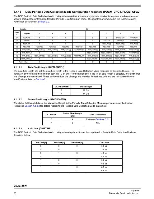
3.1.15 DSI3 Periodic <strong>Data</strong> Collection Mode Configuration registers (PDCM_CFG1, PDCM_CFG2)<br />
The DSI3 Periodic <strong>Data</strong> Collection Mode configuration registers are user programmed read/write registers which contain user<br />
specific configuration information for DSI3 Periodic <strong>Data</strong> Collection Mode. The registers are included in the read/write array<br />
verification described in Section 3.2.<br />
Addres<br />
s<br />
3.1.15.1 <strong>Data</strong> Field Length (DATALENGTH)<br />
The data field length bits set the data field length in the Periodic <strong>Data</strong> Collection Mode response as described below. The<br />
sensitivity of the data is the same for both the 10-bit and 14-bit data lengths. If the 14-bit data length is selected, four additional<br />
bits of range are transmitted. These additional four bits of range are intended for test use only and are not covered by the<br />
specifications listed in Section 2.<br />
3.1.15.2 Status Field Length (STATLENGTH)<br />
The status field length bits set the status field length in the Periodic <strong>Data</strong> Collection Mode response as described below.<br />
Reference Section 4.3.2.2 for details regarding the Periodic <strong>Data</strong> Collection Mode status field.<br />
3.1.15.3 Chip time (CHIPTIME)<br />
The DSI3 Periodic <strong>Data</strong> Collection Mode configuration chip time bits set the chip time for Periodic <strong>Data</strong> Collection Mode as<br />
described below.<br />
MMA27XXW<br />
Location Bit<br />
Register 7 6 5 4 3 2 1 0<br />
$14 PDCM_CFG 0 0 0 0 0 0 DATALENGTH STATLENGTH<br />
$16 CHIPTIME 0 0 0 0 0 CHIPTIME[2] CHIPTIME[1] CHIPTIME[0]<br />
$17 PDCM_PER 0 0 0 0 0 PDCM_PER[2] PDCM_PER[1] PDCM_PER[0]<br />
$18 RESERVED RESERVED RESERVED RESERVED RESERVED RESERVED RESERVED RESERVED RESERVED<br />
$19 PDCM_RSPST_L PDCM_RSPST[7] PDCM_RSPST[6] PDCM_RSPST[5] PDCM_RSPST[4] PDCM_RSPST[3] PDCM_RSPST[2] PDCM_RSPST[1] PDCM_RSPST[0]<br />
$1A PDCM_RSPST_H 0 0 0 0 PDCM_RSPST[11] PDCM_RSPST[10] PDCM_RSPST[9] PDCM_RSPST[8]<br />
$1B PDCM_CMD_B_L PDCM_CMD_B[7] PDCM_CMD_B[6] PDCM_CMD_B[5] PDCM_CMD_B[4] PDCM_CMD_B[3] PDCM_CMD_B[2] PDCM_CMD_B[1] PDCM_CMD_B[0]<br />
$1C PDCM_CMD_B_H 0 0 0 0 PDCM_CMD_B[11] PDCM_CMD_B[10] PDCM_CMD_B[9] PDCM_CMD_B[8]<br />
Factory Default 0 0 0 0 0 0 0 0<br />
DATALENGTH <strong>Data</strong> Length<br />
0 10 Bits<br />
1 14 Bits<br />
STATLEN<br />
Status Field Length<br />
(Bits)<br />
<strong>Data</strong> Transmitted<br />
0 4 Reference Section 4.3.2.2<br />
1 0 N/A<br />
CHIPTIME[2] CHIPTIME[1] CHIPTIME[0] Chip time<br />
0 0 0 3.0 μs<br />
0 0 1 3.5 μs<br />
0 1 0 4.0 μs<br />
0 1 1 4.5 μs<br />
1 0 0 5.0 μs<br />
1 0 1 5.5 μs<br />
1 1 0 6.0 μs<br />
1 1 1 6.5 μs<br />
Sensors<br />
20 <strong>Freescale</strong> <strong>Semiconductor</strong>, Inc.


