

Data Sheet - Freescale Semiconductor
Data Sheet - Freescale Semiconductor
Data Sheet - Freescale Semiconductor

Create successful ePaper yourself
Turn your PDF publications into a flip-book with our unique Google optimized e-Paper software.
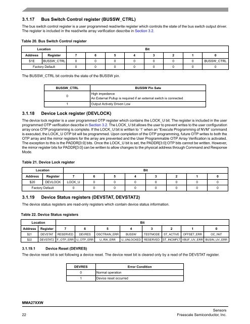
3.1.17 Bus Switch Control register (BUSSW_CTRL)<br />
The bus switch control register is a user programmed read/write register which controls the state of the bus switch output driver.<br />
The register is included in the read/write array verification describe in Section 3.2.<br />
Table 20. Bus Switch Control register<br />
Location Bit<br />
Address Register 7 6 5 4 3 2 1 0<br />
$1E BUSSW_CTRL 0 0 0 0 0 0 0 BUSSW_CTRL<br />
Factory Default 0 0 0 0 0 0 0 0<br />
The BUSSW_CTRL bit controls the state of the BUSSW pin.<br />
3.1.18 Device Lock register (DEVLOCK)<br />
The device lock register is a user programmed OTP register which contains the LOCK_U bit. The register is included in the user<br />
programmed OTP verification describe in Section 3.2. The LOCK_U bit allows the user to prevent writes to the user configuration<br />
array once OTP programming is complete. If the LOCK_U bit is written to ‘1’ when an “Execute Programming of NVM” command<br />
is executed, the LOCK_U OTP bit will be programmed. Upon completion of the OTP programming, future OTP writes to both the<br />
OTP array and the mirror registers for the array are prevented and the User Programmable OTP Array Verification is activated.<br />
The exception to this is the PADDR[3:0] bits. Once the LOCK_U bit is set, the PADDR[3:0] OTP bits cannot be written. However,<br />
the mirror register bits for PADDR[3:0] can be written to allow changes to the physical address through Command and Response<br />
Mode.<br />
Table 21. Device Lock register<br />
3.1.19 Device Status registers (DEVSTAT, DEVSTAT2)<br />
The device status registers are read-only registers which contain device status information.<br />
3.1.19.1 Device Reset (DEVRES)<br />
The device reset bit is set following a device reset. The device reset bit is cleared only by a read of the DEVSTAT register.<br />
MMA27XXW<br />
BUSSW_CTRL BUSSW Pin Sate<br />
High impedance<br />
0<br />
An External Pullup is required if an external switch is connected<br />
1 Output Actively Driven Low<br />
Location Bit<br />
Address Register 7 6 5 4 3 2 1 0<br />
$20 DEVLOCK LOCK_U 0 0 0 0 0 0 0<br />
Factory Default 0 0 0 0 0 0 0 0<br />
Table 22. Device Status registers<br />
Location Bit<br />
Address Register 7 6 5 4 3 2 1 0<br />
$21 DEVSTAT RESERVED DEVRES OSCTRAIN_ERR BUSSW TESTMODE ST_ACTIVE OFFSET_ERR OC_INIT<br />
$22 DEVSTAT2 F_OTP_ERR U_OTP_ERR U_RW_ERR U_UNLOCKED RESERVED ST_INCMPLT VBUF_UV_ERR BUSIN_UV_ERR<br />
DEVRES Error Condition<br />
0 Normal operation<br />
1 Device reset occurred<br />
Sensors<br />
22 <strong>Freescale</strong> <strong>Semiconductor</strong>, Inc.


