

Data Sheet - Freescale Semiconductor
Data Sheet - Freescale Semiconductor
Data Sheet - Freescale Semiconductor

You also want an ePaper? Increase the reach of your titles
YUMPU automatically turns print PDFs into web optimized ePapers that Google loves.
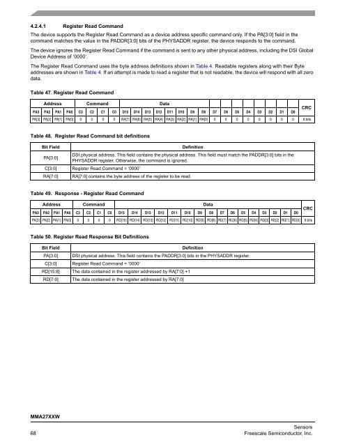
4.2.4.1 Register Read Command<br />
The device supports the Register Read Command as a device address specific command only. If the PA[3:0] field in the<br />
command matches the value in the PADDR[3:0] bits of the PHYSADDR register, the device responds to the command.<br />
The device ignores the Register Read Command if the command is sent to any other physical address, including the DSI Global<br />
Device Address of ‘0000’.<br />
The Register Read Command uses the byte address definitions shown in Table 4. Readable registers along with their Byte<br />
addresses are shown in Table 4. If an attempt is made to read a register that is not readable, the device will respond with all zero<br />
data.<br />
Table 47. Register Read Command<br />
Address Command <strong>Data</strong><br />
CRC<br />
PA3 PA2 PA1 PA0 C3 C2 C1 C0 D15 D14 D13 D12 D11 D10 D9 D8 D7 D6 D5 D4 D3 D2 D1 D0<br />
PA[3] PA[2] PA[1] PA[0] 0 0 0 0 RA[7] RA[6] RA[5] RA[4] RA[3] RA[2] RA[1] RA[0] 0 0 0 0 0 0 0 0 8 bits<br />
Table 48. Register Read Command bit definitions<br />
Bit Field Definition<br />
PA[3:0]<br />
DSI physical address. This field contains the physical address. This field must match the PADDR[3:0] bits in the<br />
PHYSADDR register. Otherwise, the command is ignored.<br />
C[3:0] Register Read Command = ‘0000’<br />
RA[7:0] RA[7:0] contains the byte address of the register to be read.<br />
Table 49. Response - Register Read Command<br />
Address Command <strong>Data</strong><br />
CRC<br />
PA3 PA2 PA1 PA0 C3 C2 C1 C0 D15 D14 D13 D12 D11 D10 D9 D8 D7 D6 D5 D4 D3 D2 D1 D0<br />
PA[3] PA[2] PA[1] PA[0] 0 0 0 0 RD[15] RD[14] RD[13] RD[12] RD[11] RD[10] RD[9] RD[8] RD[7] RD[6] RD[5] RD[4] RD[3] RD[2] RD[1] RD[0] 8 bits<br />
Table 50. Register Read Response Bit Definitions<br />
Bit Field Definition<br />
PA[3:0] DSI physical address. This field contains the PADDR[3:0] bits in the PHYSADDR register.<br />
C[3:0] Register Read Command = ‘0000’<br />
RD[15:8] The data contained in the register addressed by RA[7:0] +1<br />
RD[7:0] The data contained in the register addressed by RA[7:0]<br />
MMA27XXW<br />
Sensors<br />
68 <strong>Freescale</strong> <strong>Semiconductor</strong>, Inc.


