

Data Sheet - Freescale Semiconductor
Data Sheet - Freescale Semiconductor
Data Sheet - Freescale Semiconductor

You also want an ePaper? Increase the reach of your titles
YUMPU automatically turns print PDFs into web optimized ePapers that Google loves.
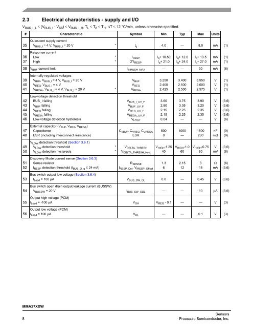
2.3 Electrical characteristics - supply and I/O<br />
V BUS_I_L ≤ (V BUS_I - V SS) ≤ V BUS_I_H, T L ≤ T A ≤ T H, ΔT ≤ 12 °C/min, unless otherwise specified.<br />
# Characteristic Symbol Min Typ Max Units<br />
35<br />
36<br />
37<br />
Quiescent supply current<br />
V BUS_I = 4 V, V BUS_I = 20 V * I q 4.0 — 8.0 mA (1)<br />
Response current<br />
Low<br />
High<br />
MMA27XXW<br />
*<br />
*<br />
IRESP 2*IRESP I q+ 10.50<br />
I q+ 21.0<br />
I q+ 12.0<br />
I q+ 24.0<br />
I q+ 13.5<br />
I q+ 27.0<br />
38 V BUF current limit I INRUSH_MAX — — 30 mA (6)<br />
39<br />
40<br />
41<br />
42<br />
43<br />
44<br />
45<br />
46<br />
47<br />
48<br />
49<br />
50<br />
51<br />
52<br />
53<br />
54<br />
55<br />
56<br />
Internally regulated voltages<br />
V BUF, V BUS_I = 4 V, V BUS_I = 20 V<br />
V REG , V BUS_I = 4 V<br />
V REGA, V BUS_I = 4 V, V BUS_I = 20 V *<br />
Low-voltage detection threshold<br />
BUS_I falling<br />
V BUF falling<br />
V REG falling<br />
V REGA falling<br />
Low-voltage detection hysteresis<br />
External capacitor (V BUF, V REG, V REGA)<br />
Capacitance<br />
ESR (including interconnect resistance)<br />
V LOW detection threshold (Section 3.6.1)<br />
V LOW detection threshold<br />
V LOW detection hysteresis<br />
Discovery Mode current sense (Section 3.6.3)<br />
Sense resistor<br />
I RESP detection threshold (I BUS_O_q ≤ 24 mA)<br />
*<br />
*<br />
V BUF<br />
V REG<br />
V REGA<br />
V BUS_I_UV_F<br />
V BUF_UV_F<br />
V REG_UV_F<br />
V REGA_UV_F<br />
V HYST<br />
C VBUF , C VREG , C VREGA<br />
ESR<br />
V DELTA_THRESH<br />
V DELTA_THRESH_Hyst<br />
RSENSE IRESP_Det, VIRESP_Offset Sensors<br />
8 <strong>Freescale</strong> <strong>Semiconductor</strong>, Inc.<br />
3.250<br />
2.400<br />
2.425<br />
3.60<br />
2.80<br />
2.15<br />
2.15<br />
0.04<br />
500<br />
0<br />
V HIGH -1.25<br />
40<br />
3.400<br />
2.500<br />
2.500<br />
3.75<br />
3.05<br />
2.25<br />
2.25<br />
—<br />
1000<br />
—<br />
V HIGH -1.0<br />
60<br />
3.550<br />
2.600<br />
2.575<br />
3.90<br />
3.20<br />
2.35<br />
2.35<br />
—<br />
1500<br />
200<br />
V HIGH -0.75<br />
80<br />
Bus switch output low voltage (Section 3.6.4)<br />
I Load = 100 μA V BUS_SW_OL 0.0 — 0.45 V (3,6)<br />
Bus switch open drain output leakage current (BUSSW)<br />
V BUSSW = 20 V I BUS_SW_ODL — — 10 μA (3,6)<br />
Output high voltage (PCM)<br />
I Load = -100 μA V OH V REG - 0.1 — — V (3)<br />
Output low voltage (PCM)<br />
I Load = 100 μA V OL — — 0.1 V (3)<br />
1.3<br />
6<br />
2.15<br />
12<br />
3<br />
18<br />
mA<br />
mA<br />
V<br />
V<br />
V<br />
V<br />
V<br />
V<br />
V<br />
V<br />
nF<br />
mΩ<br />
V<br />
mV<br />
Ω<br />
mA<br />
(1)<br />
(1)<br />
(1)<br />
(1)<br />
(1)<br />
(3,6)<br />
(3,6)<br />
(3,6)<br />
(3,6)<br />
(6)<br />
(9)<br />
(9)<br />
(3,6)<br />
(6)<br />
(6)<br />
(3,6)


