

Data Sheet - Freescale Semiconductor
Data Sheet - Freescale Semiconductor
Data Sheet - Freescale Semiconductor

You also want an ePaper? Increase the reach of your titles
YUMPU automatically turns print PDFs into web optimized ePapers that Google loves.
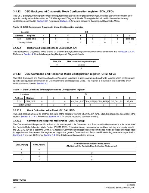
3.1.12 DSI3 Background Diagnostic Mode Configuration register (BDM_CFG)<br />
The DSI3 Background Diagnostic Mode configuration register is a user programmed read/write register which contains user<br />
specific configuration information for DSI3 Background Diagnostic Mode. The register is included in the read/write array<br />
verification described in Section 3.2. Reference Section 4.3 for details regarding Background Diagnostic Mode.<br />
Table 16. DSI3 Background Diagnostic Mode Configuration register<br />
3.1.12.1 Background Diagnostic Mode Enable (BDM_EN)<br />
The Background Diagnostic Mode enable bit enables Background Diagnostic Mode as described below and in Section 3.1.14.<br />
Reference Section 4.3 for details regarding Background Diagnostic Mode.<br />
3.1.13 DSI3 Command and Response Mode Configuration register (CRM_CFG)<br />
The DSI3 Command and Response Mode configuration register is a user programmed read/write register which contains user<br />
specific configuration information for DSI3 Command and Response Mode. The register is included in the read/write array<br />
verification described in Section 3.2.<br />
3.1.13.1 Clock Calibration Value Reset (CK_CAL_RST)<br />
The clock calibration reset bit controls the state of the oscillator training when the CK_CAL_EN bit is cleared as described in the<br />
table in Section 3.1.13.3. Reference Section 3.4.1 for details regarding oscillator training.<br />
3.1.13.2 Command and Response Mode Period (CRM_PER[1:0])<br />
The Command and Response Mode Period bits set the period for Command and Response Mode commands in increments of<br />
the Periodic <strong>Data</strong> Collection Mode Period (PDCM_PER). This value is only necessary for oscillator training and is only used if<br />
the CK_CAL_EN bit is set in the CRM_CFG register. Command and Response Mode commands will be decoded and responded<br />
to regardless of the value of this register as long as the general Command and Response Mode timing parameters specified in<br />
Section 2.6 are met. Reference Section 3.4.1 for details regarding oscillator training.<br />
MMA27XXW<br />
Location Bit<br />
Address Register 7 6 5 4 3 2 1 0<br />
$12 BDM_CFG 0 0 0 0 0 0 0 BDM_EN<br />
Factory Default 0 0 0 0 0 0 0 0<br />
BDM_EN BDM command fragment length<br />
0 Disabled<br />
1 4<br />
Table 17. DSI3 Command and Response Mode Configuration register<br />
Location Bit<br />
Address Register 7 6 5 4 3 2 1 0<br />
$13 CRM_CFG 0 0 0 CK_CAL_RST CRM_PER[1] CRM_PER[0] CK_CAL_EN SS_EN<br />
Factory Default 0 0 0 0 0 0 0 0<br />
CRM_PER[1] CRM_PER[0]<br />
Command and Response Mode period<br />
(Multiples of the Periodic <strong>Data</strong> Collection Mode period)<br />
0 0 1<br />
0 1 2<br />
1 0 4<br />
1 1 8<br />
Sensors<br />
18 <strong>Freescale</strong> <strong>Semiconductor</strong>, Inc.


