Exploration and Optimization of Tellurium‐Based Thermoelectrics
Exploration and Optimization of Tellurium‐Based Thermoelectrics
Exploration and Optimization of Tellurium‐Based Thermoelectrics

Create successful ePaper yourself
Turn your PDF publications into a flip-book with our unique Google optimized e-Paper software.
The logical rise in dimensionality that follows increasing a 0‐dimensional point defect into a 1‐D<br />
line (i.e. edge dislocation), 2‐D plane (i.e. grain boundary), or 3‐D volume (i.e. nanoregions) leads the<br />
idea <strong>of</strong> imperfections at the macro‐ <strong>and</strong> microscopic or even nanoscopic levels, driving properties such<br />
as mechanical strain or even colour. Consider for example diamonds (b<strong>and</strong> gap ~5 eV) with boron or<br />
nitrogen impurities causing blue or yellow tints from acceptor (0.4 eV) <strong>and</strong> donor (4 eV) states<br />
respectively, via energy transitions in the b<strong>and</strong> gap. [85] Examining now a 2‐dimensional defect, grain<br />
boundaries are frequently encountered in crystalline materials due to manufacturing inconsistencies,<br />
inhomogeneity in powder size, <strong>and</strong> growth in multiple directions, yielding some or all <strong>of</strong> the boundary<br />
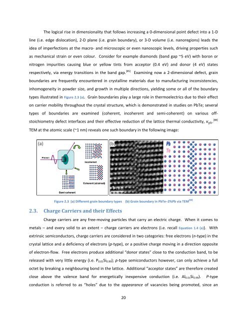
types illustrated in Figure 2.3 (a). Grain boundaries play a large role in thermoelectrics due to their effect<br />
on carrier mobility throughout the crystal structure, which is demonstrated in studies on PbTe; several<br />
types <strong>of</strong> boundaries are examined (coherent, incoherent <strong>and</strong> semi‐coherent) on various <strong>of</strong>f‐<br />
stoichiometry defect interfaces <strong>and</strong> their effective reduction <strong>of</strong> the lattice thermal conductivity, ph. [88]<br />
TEM at the atomic scale (~1 nm) reveals one such boundary in the following image:<br />
Figure 2.3 (a) Different grain boundary types (b) Grain boundary in PbTe–2%Pb via TEM [88]<br />
2.3. Charge Carriers <strong>and</strong> their Effects<br />
Charge carriers are any free‐moving particles that carry an electric charge. When it comes to<br />
metals – <strong>and</strong> every solid to an extent – charge carriers are electrons (i.e. recall Equation 1.4 (a)). With<br />
extrinsic semiconductors, charge carriers are considered in two categories: free electrons (n‐type) in the<br />
crystal lattice <strong>and</strong> a deficiency <strong>of</strong> electrons (p‐type), or a positive charge moving in a direction opposite<br />
<strong>of</strong> electron‐flow. Free electrons produce additional “donor states” close to the conduction b<strong>and</strong>, to be<br />
released with very little energy (i.e. P0.01Si0.99); p‐type semiconductors however, can only achieve a full<br />
octet by breaking a neighbouring bond in the lattice. Additional “acceptor states” are therefore created<br />
close above the valence b<strong>and</strong> for energetically inexpensive conduction (i.e. Al0.01Si0.99). P‐type<br />
conduction is referred to as “holes” due to the appearance <strong>of</strong> vacancies being promoted, since an<br />
20