Scientific Advisory Board - Erich Schmid Institute
Scientific Advisory Board - Erich Schmid Institute
Scientific Advisory Board - Erich Schmid Institute

Create successful ePaper yourself
Turn your PDF publications into a flip-book with our unique Google optimized e-Paper software.
ERICH SCHMID INSTITUTE OF MATERIALS SCIENCE<br />
was found. With all of these material and testing conditions in mind, cr and pet have been<br />
shown to be ideal materials for flexible electronics. As thin layers, less than 20nm, are typically<br />
used as adhesion layers, the 15nm cr film has exhibited ideal mechanical behavior at room<br />
temperature. All of these results indicate that the cr coated pet is a robust material system<br />
through a wide variety of mechanical testing conditions and environments illustrating its large<br />
potential for flexible electronic applications.<br />
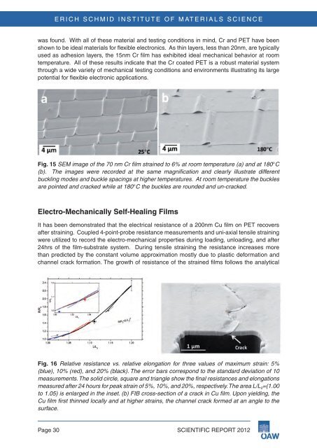
Fig . 15 SEM image of the 70 nm Cr film strained to 6% at room temperature (a) and at 180°C<br />
(b). The images were recorded at the same magnification and clearly illustrate different<br />
buckling modes and buckle spacings at higher temperatures. At room temperature the buckles<br />
are pointed and cracked while at 180°C the buckles are rounded and un-cracked.<br />
Electro-Mechanically Self-Healing Films<br />
it has been demonstrated that the electrical resistance of a 200nm cu film on pet recovers<br />
after straining. coupled 4-point-probe resistance measurements and uni-axial tensile straining<br />
were utilized to record the electro-mechanical properties during loading, unloading, and after<br />
24hrs of the film-substrate system. during tensile straining the resistance increases more<br />
than predicted by the constant volume approximation mostly due to plastic deformation and<br />
channel crack formation. the growth of resistance of the strained films follows the analytical<br />
Fig . 16 Relative resistance vs. relative elongation for three values of maximum strain: 5%<br />
(blue), 10% (red), and 20% (black). The error bars correspond to the standard deviation of 10<br />
measurements. The solid circle, square and triangle show the final resistances and elongations<br />
measured after 24 hours for peak strain of 5%, 10%, and 20%, respectively. The area L/L 0=(1.00<br />
to 1.05) is enlarged in the inset. (b) FIB cross-section of a crack in Cu film. Upon yielding, the<br />
Cu film first thinned locally and at higher strains, the channel crack formed at an angle to the<br />
surface.<br />
page 30 <strong>Scientific</strong> RepoRt 2012