PcB - High Frequency Electronics
PcB - High Frequency Electronics
PcB - High Frequency Electronics

Create successful ePaper yourself
Turn your PDF publications into a flip-book with our unique Google optimized e-Paper software.
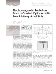
<strong>High</strong> <strong>Frequency</strong> Design<br />
PCB Probing<br />
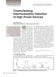
This is best illustrated by looking in the time domain<br />
to see the full path of discontinuities when measured<br />
with a VNA NIST traceable automated electronic E-CAL<br />
calibration. Figure 8 shows this full path in blue with<br />
both the coaxial 2.4 mm adapter and the Probe Interposer<br />
impedance variations. The coaxial 2.4 mm to PCB adapter<br />
portion is characterized by selecting the coax 2.4mm<br />
reference plane for Port 1 and the bottom of the Probe<br />
Interposer TRL reference plane for Port 2. The coaxial<br />
2.4mm to PCB adapter going to the Probe Interposer is<br />
then defined as the adapter going from Port 1 to Port 2 in<br />
the VNA TRL with Adapter Removal calibration.<br />
The resulting measurement in green in Figure 8<br />
shows just the impedance and electrical length of the<br />
coaxial 2.4 mm connector to PCB fixturing. This is then<br />
de-embedded from the full path measurement in blue to<br />
end up with just the electrical performance of the Probe<br />
Interposer shown in red. Making use of automated electronic<br />
coaxial calibrations and batched file de-embedding<br />
of the fixture significantly reduces connector repeatability<br />
and human errors that are always a challenge with<br />
high port count calibrations and measurements.<br />
Symmetrical 2x Through Calibration (AFR)<br />
The previous section showed how TRL calibration<br />
standards can provide a method of calibrating to a reference<br />
plane that is vertically located relative to the planar<br />
PCB surface. The use of the horizontal microstrip connection<br />
to the bottom of the Probe Interposer does simplify<br />
the creation of the multiple line lengths for the TRL calibration<br />
standards, but does not exactly replicate the vertical<br />
connection that the Probe Interposer makes to the<br />
PCB BGA interface or BGA socket. An alternative<br />
method is to make use of calibration techniques that only<br />
require a single symmetrical through path where half of<br />
the path is the desired electrical fixture and the length is<br />
2 times the fixture length x, hence the name “2x Through”<br />
calibration standard [3].<br />
The 2x Through path is simply created by connecting<br />
two symmetrical Probe Interposers together as shown in<br />
Figure 9. The electrical connection between the two contacting<br />
surfaces can be improved with a thin vertical<br />
interconnect material such as Paricon’s Pariposer material<br />
[8]. If a BGA socket is used between the two Probe<br />
Figure 10 • Alternative AFR calibration using a 2x<br />
through path to measure the Probe Interposer.<br />
Interposers then the reference plane can be placed in the<br />
middle of the socket. This alternative method does<br />
require two sided probing and the need for mirror image<br />
PCB interposers to enable back to back connection of the<br />
signal and ground BGA ball-out connections.<br />
Implementing a second calibration technique also<br />
provides another level of confidence and understanding of<br />
how sensitive the reference plane is for a particular measurement<br />
location. The measurements for the back-toback<br />
probe interposer with and without the BGA socket<br />
were done with an automated E-Cal calibration to the<br />
ends of the VNA coaxial cables, and then Agilent’s PLTS<br />
software provides the Automatic Fixture Removal (AFR)<br />
algorithm for splitting the measurement of the 2x<br />
through standard into two parts for de-embedding of the<br />
fixture from the VNA measurement.<br />
The AFR 2x through measurement results in Figure<br />
10 reconfirm the wide bandwidth performance of the<br />
Probe Interposer that were measured with the TRL standards.<br />
Using this technique one can also include the BGA<br />
socket and place the reference plane in the middle of the<br />
pogo pins in the vertical direction. The resulting data<br />
shown in blue in Figure 10 demonstrates that the Probe<br />
Interposer to BGA socket transition has little degradation<br />
on the bandwidth and that the Probe Interposer<br />
design provides a robust connection to the BGA socket.<br />
Multi-port Crosstalk Measurements with Fixture Removal<br />
Now, with the Probe Interposer design verified and<br />
multiple probe interposer fixtures characterized it is time<br />
Figure 9 • Two sided probing measurement of the 2x<br />
through path with back to back Probe Interposers on<br />
the left, and with the BGA socket added on the right.<br />
30 <strong>High</strong> <strong>Frequency</strong> <strong>Electronics</strong><br />
Figure 11 • 12-Port VNA measurement of 6 ATE DUT<br />
Board signal paths with 6 adjacent Probe Interposer<br />
connections fanning out to 6 SMA connections.